- 您現(xiàn)在的位置:買(mǎi)賣(mài)IC網(wǎng) > PDF目錄373358 > S9840 (Hamamatsu Photonics) High UV sensitivity CCD image sensor PDF資料下載
參數(shù)資料
| 型號(hào): | S9840 |
| 廠商: | Hamamatsu Photonics |
| 英文描述: | High UV sensitivity CCD image sensor |
| 中文描述: | 高靈敏度紫外CCD圖像傳感器 |
| 文件頁(yè)數(shù): | 4/4頁(yè) |
| 文件大?。?/td> | 92K |
| 代理商: | S9840 |
CCD image sensor
S9840
HAMAMATSU PHOTONICS K.K., Solid State Division
1126-1 Ichino-cho, Higashi-ku, Hamamatsu City, 435-8558 Japan, Telephone: (81) 53-434-3311, Fax: (81) 53-434-5184, www.hamamatsu.com
U.S.A.: Hamamatsu Corporation: 360 Foothill Road, P.O.Box 6910, Bridgewater, N.J. 08807-0910, U.S.A., Telephone: (1) 908-231-0960, Fax: (1) 908-231-1218
Germany: Hamamatsu Photonics Deutschland GmbH: Arzbergerstr. 10, D-82211 Herrsching am Ammersee, Germany, Telephone: (49) 08152-3750, Fax: (49) 08152-2658
France: Hamamatsu Photonics France S.A.R.L.: 19, Rue du Saule Trapu, Parc du Moulin de Massy, 91882 Massy Cedex, France, Telephone: 33-(1) 69 53 71 00, Fax: 33-(1) 69 53 71 10
United Kingdom: Hamamatsu Photonics UK Limited: 2 Howard Court, 10 Tewin Road, Welwyn Garden City, Hertfordshire AL7 1BW, United Kingdom, Telephone: (44) 1707-294888, Fax: (44) 1707-325777
North Europe: Hamamatsu Photonics Norden AB: Smidesv
gen 12, SE-171 41 Solna, Sweden, Telephone: (46) 8-509-031-00, Fax: (46) 8-509-031-01
Italy: Hamamatsu Photonics Italia S.R.L.: Strada della Moia, 1/E, 20020 Arese, (Milano), Italy, Telephone: (39) 02-935-81-733, Fax: (39) 02-935-81-741
Information furnished by HAMAMATSU is believed to be reliable. However, no responsibility is assumed for possible inaccuracies or omissions.
Specifications are subject to change without notice. No patent rights are granted to any of the circuits described herein. 2007 Hamamatsu Photonics K.K.
Cat. No. KMPD1082E09
Aug. 2007 DN
4
I
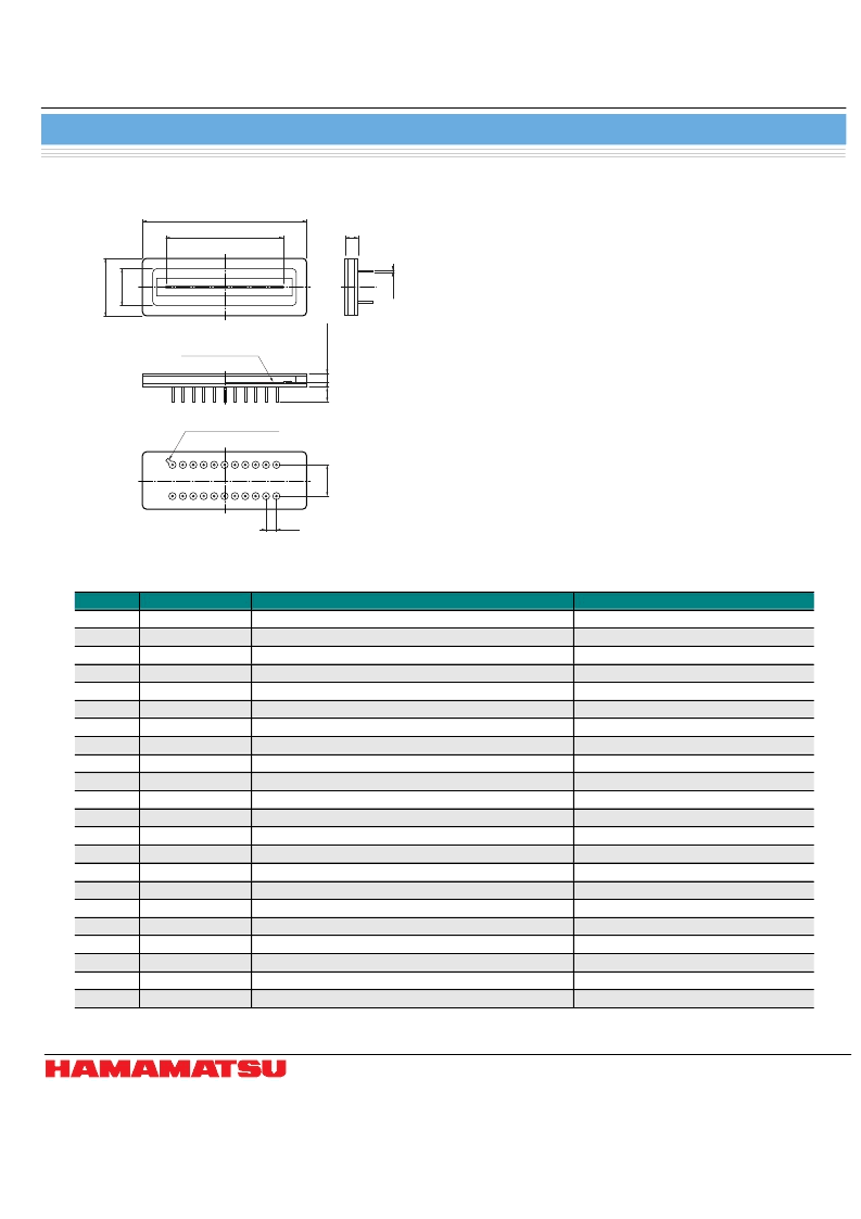
Dimensional outline (unit: mm)
ACTIVE AREA 28.672
3.1
± 0.25
0
9
2
±
3
PHOTOSENSITIVE
SURFACE
7
2.54
A1
B1
A11
B11
INDEX MARK PIN No. 1
* Distance between window surface and photosensitive surface
1
+
-
40.0
-0.4
KMPDA0186ED
I
Pin connections
Pin No.
A1
A2
A3
A4
A5
A6
A7
A8
A9
A10
A11
B1
B2
B3
B4
B5
B6
B7
B8
B9
B10
B11
*6: Isolation gate between vertical register and horizontal register. In standard operation, TG should be applied the same pulse as
P2V.
Symbol
OS
OD
SS
RD
RG
OG
OFD
OFG
P2H
P1H
ISH
SG
P2V
P1V
TG *
6
-
-
RD
SS
P1V
P2V
IGH
Function
Remark (standard operation)
Output signal
DC (+20 V)
GND
DC (+12 V)
Clock (+6/-8 V)
DC (+3 V)
DC (+12 V)
Same pulse as P1H
Clock (+6/-8 V)
Clock (+6/-8 V)
DC (+12 V)
Same pulse as P2H
Clock (+6/-8 V)
Clock (+6/-8 V)
Same pulse as P2V
-
-
DC (+12 V)
GND
Clock (+6/-8 V)
Clock (+6/-8 V)
GND
Output transistor source, internal R
L
Output transistor drain
Substrate (GND)
Reset drain
Reset gate
Output gate
Output flow drain
Output flow gate
CCD horizontal register clock-2
CCD horizontal resister clock-1
Test point (input source)
Summing gate
CCD vertical register clock-2
CCD vertical register clock-1
Transfer gate
-
-
Reset drain
Substrate (GND)
CCD vertical register clock-1
CCD vertical register clock-2
Test point (input gate)
相關(guān)PDF資料 |
PDF描述 |
|---|---|
| S9970 | CCD area image sensor Low dark signal · low readout noise/front-illuminated FFT-CCD |
| S9970-0906 | CCD area image sensor Low dark signal · low readout noise/front-illuminated FFT-CCD |
| S9970-1006 | Diode; Detector and mixer; VR (V): [25]; IF (mA): -; Pd (mW): -; rf (ohm) max: -; Condition IF at rf (mA): -; Condition f at rf (MHz): -; VF (V) max: 0.33; Condition IF at VF (mA): 1; C (pF) max: 2.8; Condition VR at C (V): 1; Condition f at C (MHz): 1; Package: EFP |
| S9970-1007 | CCD area image sensor Low dark signal · low readout noise/front-illuminated FFT-CCD |
| S9970-1008 | CCD area image sensor Low dark signal · low readout noise/front-illuminated FFT-CCD |
相關(guān)代理商/技術(shù)參數(shù) |
參數(shù)描述 |
|---|---|
| S984-SP | 制造商:Cooper Wiring Devices 功能描述: |
| S987DC3-2 | 制造商:NUTS 功能描述: |
| S987DC3-3 | 制造商:NUTS 功能描述: |
| S987-RAAF5-632 | 制造商:MISCELLANEOUS 功能描述: |
| S989-10-020-00-350200 | 制造商:MILL-MAX 功能描述: 制造商:Mill-Max Mfg Corp 功能描述: |
發(fā)布緊急采購(gòu),3分鐘左右您將得到回復(fù)。