- 您現(xiàn)在的位置:買賣IC網(wǎng) > PDF目錄25642 > S80C32-L16SHXXX (ATMEL CORP) 8-BIT, 16 MHz, MICROCONTROLLER, PQCC44 PDF資料下載
參數(shù)資料
| 型號: | S80C32-L16SHXXX |
| 廠商: | ATMEL CORP |
| 元件分類: | 微控制器/微處理器 |
| 英文描述: | 8-BIT, 16 MHz, MICROCONTROLLER, PQCC44 |
| 封裝: | PLASTIC, LCC-44 |
| 文件頁數(shù): | 226/313頁 |
| 文件大小: | 4988K |
| 代理商: | S80C32-L16SHXXX |
第1頁第2頁第3頁第4頁第5頁第6頁第7頁第8頁第9頁第10頁第11頁第12頁第13頁第14頁第15頁第16頁第17頁第18頁第19頁第20頁第21頁第22頁第23頁第24頁第25頁第26頁第27頁第28頁第29頁第30頁第31頁第32頁第33頁第34頁第35頁第36頁第37頁第38頁第39頁第40頁第41頁第42頁第43頁第44頁第45頁第46頁第47頁第48頁第49頁第50頁第51頁第52頁第53頁第54頁第55頁第56頁第57頁第58頁第59頁第60頁第61頁第62頁第63頁第64頁第65頁第66頁第67頁第68頁第69頁第70頁第71頁第72頁第73頁第74頁第75頁第76頁第77頁第78頁第79頁第80頁第81頁第82頁第83頁第84頁第85頁第86頁第87頁第88頁第89頁第90頁第91頁第92頁第93頁第94頁第95頁第96頁第97頁第98頁第99頁第100頁第101頁第102頁第103頁第104頁第105頁第106頁第107頁第108頁第109頁第110頁第111頁第112頁第113頁第114頁第115頁第116頁第117頁第118頁第119頁第120頁第121頁第122頁第123頁第124頁第125頁第126頁第127頁第128頁第129頁第130頁第131頁第132頁第133頁第134頁第135頁第136頁第137頁第138頁第139頁第140頁第141頁第142頁第143頁第144頁第145頁第146頁第147頁第148頁第149頁第150頁第151頁第152頁第153頁第154頁第155頁第156頁第157頁第158頁第159頁第160頁第161頁第162頁第163頁第164頁第165頁第166頁第167頁第168頁第169頁第170頁第171頁第172頁第173頁第174頁第175頁第176頁第177頁第178頁第179頁第180頁第181頁第182頁第183頁第184頁第185頁第186頁第187頁第188頁第189頁第190頁第191頁第192頁第193頁第194頁第195頁第196頁第197頁第198頁第199頁第200頁第201頁第202頁第203頁第204頁第205頁第206頁第207頁第208頁第209頁第210頁第211頁第212頁第213頁第214頁第215頁第216頁第217頁第218頁第219頁第220頁第221頁第222頁第223頁第224頁第225頁當前第226頁第227頁第228頁第229頁第230頁第231頁第232頁第233頁第234頁第235頁第236頁第237頁第238頁第239頁第240頁第241頁第242頁第243頁第244頁第245頁第246頁第247頁第248頁第249頁第250頁第251頁第252頁第253頁第254頁第255頁第256頁第257頁第258頁第259頁第260頁第261頁第262頁第263頁第264頁第265頁第266頁第267頁第268頁第269頁第270頁第271頁第272頁第273頁第274頁第275頁第276頁第277頁第278頁第279頁第280頁第281頁第282頁第283頁第284頁第285頁第286頁第287頁第288頁第289頁第290頁第291頁第292頁第293頁第294頁第295頁第296頁第297頁第298頁第299頁第300頁第301頁第302頁第303頁第304頁第305頁第306頁第307頁第308頁第309頁第310頁第311頁第312頁第313頁
325
SAM9X25 [DATASHEET]
11054E–ATARM–10-Mar-2014
26.4 I/O Lines Description
The connection of some signals through the MUX logic is not direct and depends on the Memory Controller in use at the
moment.
Table 26-2 details the connections between the two Memory Controllers and the EBI pins.
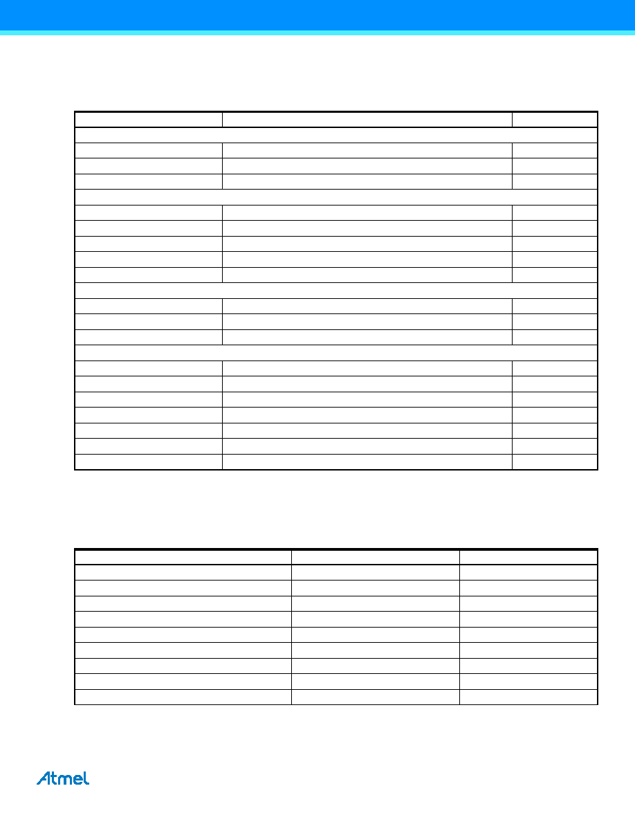
Table 26-1. EBI I/O Lines Description
Name
Function
Type
Active Level
EBI
EBI_D0–EBI_D31
Data Bus
I/O
EBI_A0–EBI_A25
Address Bus
Output
EBI_NWAIT
External Wait Signal
Input
Low
SMC
EBI_NCS0–EBI_NCS5
Chip Select Lines
Output
Low
EBI_NWR0–EBI_NWR3
Write Signals
Output
Low
EBI_NRD
Read Signal
Output
Low
EBI_NWE
Write Enable
Output
Low
EBI_NBS0–EBI_NBS3
Byte Mask Signals
Output
Low
EBI for NAND Flash Support
EBI_NANDCS
NAND Flash Chip Select Line
Output
Low
EBI_NANDOE
NAND Flash Output Enable
Output
Low
EBI_NANDWE
NAND Flash Write Enable
Output
Low
DDR2/SDRAM Controller
EBI_SDCK, EBI_SDCK#
DDR2/SDRAM Differential Clock
Output
EBI_SDCKE
DDR2/SDRAM Clock Enable
Output
High
EBI_SDCS
DDR2/SDRAM Controller Chip Select Line
Output
Low
EBI_BA0–2
Bank Select
Output
EBI_SDWE
DDR2/SDRAM Write Enable
Output
Low
EBI_RAS - EBI_CAS
Row and Column Signal
Output
Low
EBI_SDA10
SDRAM Address 10 Line
Output
Table 26-2. EBI Pins and Memory Controllers I/O Lines Connections
EBIx Pins
SDRAM I/O Lines
SMC I/O Lines
EBI_NWR1/NBS1/CFIOR
NBS1
NWR1
EBI_A0/NBS0
Not Supported
SMC_A0
EBI_A1/NBS2/NWR2
Not Supported
SMC_A1
EBI_A[11:2]
SDRAMC_A[9:0]
SMC_A[11:2]
EBI_SDA10
SDRAMC_A10
Not Supported
EBI_A12
Not Supported
SMC_A12
EBI_A[15:13]
SDRAMC_A[13:11]
SMC_A[15:13]
EBI_A[25:16]
Not Supported
SMC_A[25:16]
EBI_D[31:0]
D[31:0]
相關PDF資料 |
PDF描述 |
|---|---|
| S8890-15 | AVALANCHE PHOTO DIODE |
| S908QC16CDRER | 8-BIT, FLASH, 8 MHz, MICROCONTROLLER, PDSO28 |
| MC908QC16CDRE | 8-BIT, FLASH, 8 MHz, MICROCONTROLLER, PDSO28 |
| MC908QC16CDTE | 8-BIT, FLASH, 8 MHz, MICROCONTROLLER, PDSO16 |
| S912XDP512F0VPV | 16-BIT, FLASH, 40 MHz, MICROCONTROLLER, PQFP112 |
相關代理商/技術參數(shù) |
參數(shù)描述 |
|---|---|
| S80C376CB8 WAF | 制造商:Intel 功能描述: |
| S80C42 | 制造商:Intel 功能描述: |
| S80C51 WAF | 制造商:Intel 功能描述: |
| S80C51-12 | 制造商:未知廠家 制造商全稱:未知廠家 功能描述:8-Bit Microcontroller |
| S80C51-16 | 制造商:未知廠家 制造商全稱:未知廠家 功能描述:8-Bit Microcontroller |
發(fā)布緊急采購,3分鐘左右您將得到回復。