- 您現(xiàn)在的位置:買賣IC網(wǎng) > PDF目錄225144 > S71PL032J80BFW054 (SPANSION LLC) SPECIALTY MEMORY CIRCUIT, PBGA56 PDF資料下載
參數(shù)資料
| 型號(hào): | S71PL032J80BFW054 |
| 廠商: | SPANSION LLC |
| 元件分類: | 存儲(chǔ)器 |
| 英文描述: | SPECIALTY MEMORY CIRCUIT, PBGA56 |
| 封裝: | 7 X 9 MM, 1.20 MM HEIGHT, LEAD FREE, FBGA-56 |
| 文件頁(yè)數(shù): | 51/188頁(yè) |
| 文件大?。?/td> | 5078K |
| 代理商: | S71PL032J80BFW054 |
第1頁(yè)第2頁(yè)第3頁(yè)第4頁(yè)第5頁(yè)第6頁(yè)第7頁(yè)第8頁(yè)第9頁(yè)第10頁(yè)第11頁(yè)第12頁(yè)第13頁(yè)第14頁(yè)第15頁(yè)第16頁(yè)第17頁(yè)第18頁(yè)第19頁(yè)第20頁(yè)第21頁(yè)第22頁(yè)第23頁(yè)第24頁(yè)第25頁(yè)第26頁(yè)第27頁(yè)第28頁(yè)第29頁(yè)第30頁(yè)第31頁(yè)第32頁(yè)第33頁(yè)第34頁(yè)第35頁(yè)第36頁(yè)第37頁(yè)第38頁(yè)第39頁(yè)第40頁(yè)第41頁(yè)第42頁(yè)第43頁(yè)第44頁(yè)第45頁(yè)第46頁(yè)第47頁(yè)第48頁(yè)第49頁(yè)第50頁(yè)當(dāng)前第51頁(yè)第52頁(yè)第53頁(yè)第54頁(yè)第55頁(yè)第56頁(yè)第57頁(yè)第58頁(yè)第59頁(yè)第60頁(yè)第61頁(yè)第62頁(yè)第63頁(yè)第64頁(yè)第65頁(yè)第66頁(yè)第67頁(yè)第68頁(yè)第69頁(yè)第70頁(yè)第71頁(yè)第72頁(yè)第73頁(yè)第74頁(yè)第75頁(yè)第76頁(yè)第77頁(yè)第78頁(yè)第79頁(yè)第80頁(yè)第81頁(yè)第82頁(yè)第83頁(yè)第84頁(yè)第85頁(yè)第86頁(yè)第87頁(yè)第88頁(yè)第89頁(yè)第90頁(yè)第91頁(yè)第92頁(yè)第93頁(yè)第94頁(yè)第95頁(yè)第96頁(yè)第97頁(yè)第98頁(yè)第99頁(yè)第100頁(yè)第101頁(yè)第102頁(yè)第103頁(yè)第104頁(yè)第105頁(yè)第106頁(yè)第107頁(yè)第108頁(yè)第109頁(yè)第110頁(yè)第111頁(yè)第112頁(yè)第113頁(yè)第114頁(yè)第115頁(yè)第116頁(yè)第117頁(yè)第118頁(yè)第119頁(yè)第120頁(yè)第121頁(yè)第122頁(yè)第123頁(yè)第124頁(yè)第125頁(yè)第126頁(yè)第127頁(yè)第128頁(yè)第129頁(yè)第130頁(yè)第131頁(yè)第132頁(yè)第133頁(yè)第134頁(yè)第135頁(yè)第136頁(yè)第137頁(yè)第138頁(yè)第139頁(yè)第140頁(yè)第141頁(yè)第142頁(yè)第143頁(yè)第144頁(yè)第145頁(yè)第146頁(yè)第147頁(yè)第148頁(yè)第149頁(yè)第150頁(yè)第151頁(yè)第152頁(yè)第153頁(yè)第154頁(yè)第155頁(yè)第156頁(yè)第157頁(yè)第158頁(yè)第159頁(yè)第160頁(yè)第161頁(yè)第162頁(yè)第163頁(yè)第164頁(yè)第165頁(yè)第166頁(yè)第167頁(yè)第168頁(yè)第169頁(yè)第170頁(yè)第171頁(yè)第172頁(yè)第173頁(yè)第174頁(yè)第175頁(yè)第176頁(yè)第177頁(yè)第178頁(yè)第179頁(yè)第180頁(yè)第181頁(yè)第182頁(yè)第183頁(yè)第184頁(yè)第185頁(yè)第186頁(yè)第187頁(yè)第188頁(yè)
146
SRAM
SRAM_Type01_02A0 June 15, 2004
Prelimin ary
SRAM
4/8 Megabit CMOS SRAM
Common Features
Process Technology: Full CMOS
Power Supply Voltage: 2.7~3.3V
Three state outputs
Notes:
1. UB#, LB# swapping is available only at x16. x8 or x16 select by BYTE# pin.
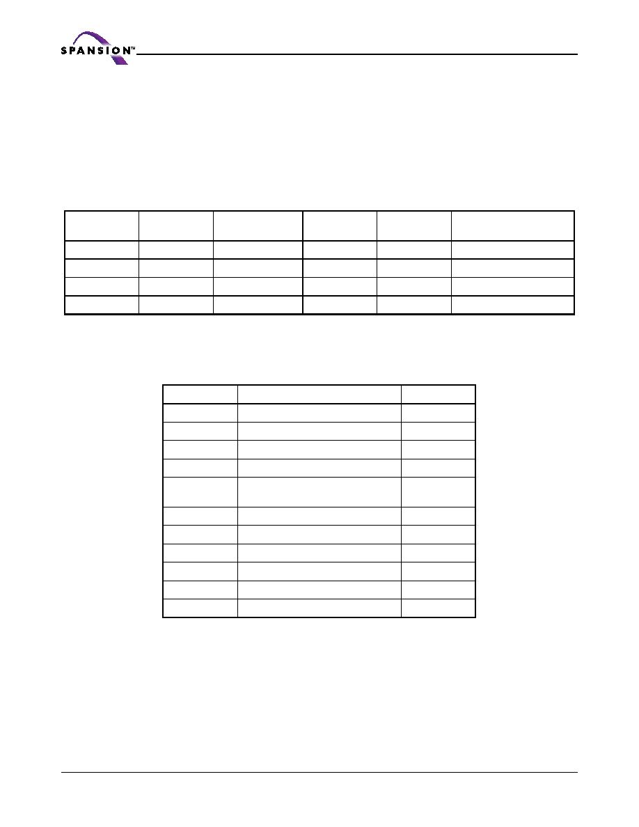
Pin Description
Version
Density
Organization
(ISB1, Max.)
Standby
(ICC2, Max.)
Operating
Mode
F
4Mb
x8 or x16 (note 1)
10 A
22 mA
Dual CS, UB# / LB# (tCS)
G
4Mb
x8 or x16 (note 1)
10 A
22 mA
Dual CS, UB# / LB# (tCS)
C
8Mb
x8 or x16 (note 1)
15 A
22 mA
Dual CS, UB# / LB# (tCS)
D
8Mb
X16
TBD
Dual CS, UB# / LB# (tCS)
Pin Name
Description
I/O
CS1#, CS2
Chip Selects
I
OE#
Output Enable
I
WE#
Write Enable
I
BYTE#
Word (VCC)/Byte (VSS) Select
I
A0~A17 (4M)
A0~A18 (8M)
Address Inputs
I
SA
Address Input for Byte Mode
I
I/O0~I/O15
Data Inputs/Outputs
I/O
VCC
Power Supply
-
VSS
Ground
-
DNU
Do Not Use
-
NC
No Connection
-
相關(guān)PDF資料 |
PDF描述 |
|---|---|
| S72NS128RD0AHBG40 | SPECIALTY MEMORY CIRCUIT, PBGA133 |
| S72NS128RD0AHBL00 | SPECIALTY MEMORY CIRCUIT, PBGA133 |
| S75PL127JCFBFWB0 | Power supply woltage of 2.7 to 3.1 volt |
| S75PL127JCFBFWB3 | Power supply woltage of 2.7 to 3.1 volt |
| S75PL127JCFBFWU0 | Power supply woltage of 2.7 to 3.1 volt |
相關(guān)代理商/技術(shù)參數(shù) |
參數(shù)描述 |
|---|---|
| S71PL032J80BFW0Z0 | 制造商:SPANSION 制造商全稱:SPANSION 功能描述:Based MCPs |
| S71PL032J80BFW0Z2 | 制造商:SPANSION 制造商全稱:SPANSION 功能描述:Based MCPs |
| S71PL032J80BFW0Z3 | 制造商:SPANSION 制造商全稱:SPANSION 功能描述:Based MCPs |
| S71PL032J80BFW9Z0 | 制造商:SPANSION 制造商全稱:SPANSION 功能描述:Based MCPs |
| S71PL032J80BFW9Z2 | 制造商:SPANSION 制造商全稱:SPANSION 功能描述:Based MCPs |
發(fā)布緊急采購(gòu),3分鐘左右您將得到回復(fù)。