- 您現(xiàn)在的位置:買(mǎi)賣(mài)IC網(wǎng) > PDF目錄192305 > S71GL064A08BAW0F3 (SPANSION LLC) Stacked Multi-Chip Product (MCP) Flash Memory and RAM PDF資料下載
參數(shù)資料
| 型號(hào): | S71GL064A08BAW0F3 |
| 廠商: | SPANSION LLC |
| 元件分類(lèi): | 存儲(chǔ)器 |
| 英文描述: | Stacked Multi-Chip Product (MCP) Flash Memory and RAM |
| 中文描述: | SPECIALTY MEMORY CIRCUIT, PBGA56 |
| 封裝: | 7 X 9 MM, 1.20 MM HEIGHT, LEAD FREE, FBGA-56 |
| 文件頁(yè)數(shù): | 83/134頁(yè) |
| 文件大小: | 2383K |
| 代理商: | S71GL064A08BAW0F3 |
第1頁(yè)第2頁(yè)第3頁(yè)第4頁(yè)第5頁(yè)第6頁(yè)第7頁(yè)第8頁(yè)第9頁(yè)第10頁(yè)第11頁(yè)第12頁(yè)第13頁(yè)第14頁(yè)第15頁(yè)第16頁(yè)第17頁(yè)第18頁(yè)第19頁(yè)第20頁(yè)第21頁(yè)第22頁(yè)第23頁(yè)第24頁(yè)第25頁(yè)第26頁(yè)第27頁(yè)第28頁(yè)第29頁(yè)第30頁(yè)第31頁(yè)第32頁(yè)第33頁(yè)第34頁(yè)第35頁(yè)第36頁(yè)第37頁(yè)第38頁(yè)第39頁(yè)第40頁(yè)第41頁(yè)第42頁(yè)第43頁(yè)第44頁(yè)第45頁(yè)第46頁(yè)第47頁(yè)第48頁(yè)第49頁(yè)第50頁(yè)第51頁(yè)第52頁(yè)第53頁(yè)第54頁(yè)第55頁(yè)第56頁(yè)第57頁(yè)第58頁(yè)第59頁(yè)第60頁(yè)第61頁(yè)第62頁(yè)第63頁(yè)第64頁(yè)第65頁(yè)第66頁(yè)第67頁(yè)第68頁(yè)第69頁(yè)第70頁(yè)第71頁(yè)第72頁(yè)第73頁(yè)第74頁(yè)第75頁(yè)第76頁(yè)第77頁(yè)第78頁(yè)第79頁(yè)第80頁(yè)第81頁(yè)第82頁(yè)當(dāng)前第83頁(yè)第84頁(yè)第85頁(yè)第86頁(yè)第87頁(yè)第88頁(yè)第89頁(yè)第90頁(yè)第91頁(yè)第92頁(yè)第93頁(yè)第94頁(yè)第95頁(yè)第96頁(yè)第97頁(yè)第98頁(yè)第99頁(yè)第100頁(yè)第101頁(yè)第102頁(yè)第103頁(yè)第104頁(yè)第105頁(yè)第106頁(yè)第107頁(yè)第108頁(yè)第109頁(yè)第110頁(yè)第111頁(yè)第112頁(yè)第113頁(yè)第114頁(yè)第115頁(yè)第116頁(yè)第117頁(yè)第118頁(yè)第119頁(yè)第120頁(yè)第121頁(yè)第122頁(yè)第123頁(yè)第124頁(yè)第125頁(yè)第126頁(yè)第127頁(yè)第128頁(yè)第129頁(yè)第130頁(yè)第131頁(yè)第132頁(yè)第133頁(yè)第134頁(yè)
50
S71GL064A based MCPs
S71GL064A_00_A2 February 8, 2005
Advance
Info rmation
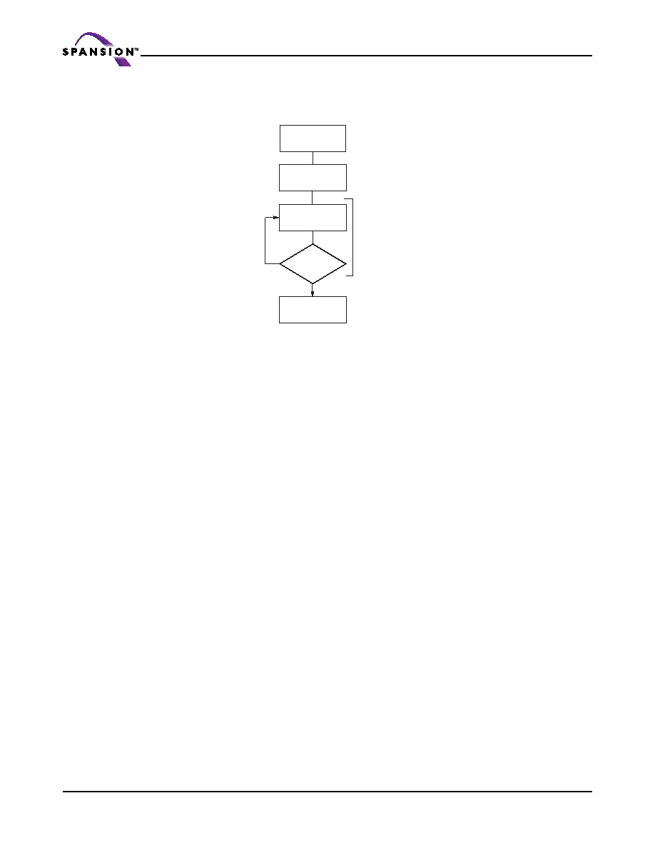
Figure 6 illustrates the algorithm for the erase operation. Refer to the Erase and Program Op-
erations table in the AC Characteristics section for parameters, and Figure 18 section for
timing diagrams.
Notes:
1. See Table 10 for program command sequence.
2. See the section on DQ3 for information on the sector erase timer.
Figure 6. Erase Operation
Erase Suspend/Erase Resume Commands
The Erase Suspend command, B0h, allows the system to interrupt a sector erase operation
and then read data from, or program data to, any sector not selected for erasure. This com-
mand is valid only during the sector erase operation, including the 50 s time-out period
during the sector erase command sequence. The Erase Suspend command is ignored if writ-
ten during the chip erase operation or Embedded Program algorithm.
When the Erase Suspend command is written during the sector erase operation, the device
requires a typical of 5 s (maximum of 20 s) to suspend the erase operation. However, when
the Erase Suspend command is written during the sector erase time-out, the device immedi-
ately terminates the time-out period and suspends the erase operation.
After the erase operation has been suspended, the device enters the erase-suspend-read
mode. The system can read data from or program data to any sector not selected for erasure.
(The device “erase suspends” all sectors selected for erasure.) Reading at any address within
erase-suspended sectors produces status information on DQ7–DQ0. The system can use
DQ7, or DQ6 and DQ2 together, to determine if a sector is actively erasing or is erase-sus-
pended. Refer to the Write Operation Status section for information on these status bits.
After an erase-suspended program operation is complete, the device returns to the erase-
suspend-read mode. The system can determine the status of the program operation using the
DQ7 or DQ6 status bits, just as in the standard word program operation. Refer to the Write
Operation Status section for more information.
In the erase-suspend-read mode, the system can also issue the autoselect command se-
quence. Refer to the “Autoselect Mode” section on page 29 and “Autoselect Command
Sequence” section on page 41 sections for details.
To resume the sector erase operation, the system must write the Erase Resume command.
Further writes of the Resume command are ignored. Another Erase Suspend command can
be written after the chip has resumed erasing.
START
Write Erase
Command Sequence
(Notes 1, 2)
Data Poll to Erasing
Bank from System
Data = FFh?
No
Yes
Erasure Completed
Embedded
Erase
algorithm
in progress
相關(guān)PDF資料 |
PDF描述 |
|---|---|
| S71GL064A08BFI0B2 | Stacked Multi-Chip Product (MCP) Flash Memory and RAM |
| S71GL064A08BFI0B3 | Stacked Multi-Chip Product (MCP) Flash Memory and RAM |
| S71GL064A08BFI0F3 | Stacked Multi-Chip Product (MCP) Flash Memory and RAM |
| S71GL064A08BFW0B2 | Stacked Multi-Chip Product (MCP) Flash Memory and RAM |
| S71GL064A08BFW0B3 | Stacked Multi-Chip Product (MCP) Flash Memory and RAM |
相關(guān)代理商/技術(shù)參數(shù) |
參數(shù)描述 |
|---|---|
| S71GL064A08BFI0B0 | 制造商:SPANSION 制造商全稱(chēng):SPANSION 功能描述:Stacked Multi-Chip Product (MCP) Flash Memory and RAM |
| S71GL064A08BFI0B2 | 制造商:SPANSION 制造商全稱(chēng):SPANSION 功能描述:Stacked Multi-Chip Product (MCP) Flash Memory and RAM |
| S71GL064A08BFI0B3 | 制造商:SPANSION 制造商全稱(chēng):SPANSION 功能描述:Stacked Multi-Chip Product (MCP) Flash Memory and RAM |
| S71GL064A08BFI0F0 | 制造商:SPANSION 制造商全稱(chēng):SPANSION 功能描述:Stacked Multi-Chip Product (MCP) Flash Memory and RAM |
| S71GL064A08BFI0F2 | 制造商:SPANSION 制造商全稱(chēng):SPANSION 功能描述:Stacked Multi-Chip Product (MCP) Flash Memory and RAM |
發(fā)布緊急采購(gòu),3分鐘左右您將得到回復(fù)。