- 您現(xiàn)在的位置:買賣IC網(wǎng) > PDF目錄373335 > RX5500-1 Analog IC PDF資料下載
參數(shù)資料
| 型號: | RX5500-1 |
| 英文描述: | Analog IC |
| 中文描述: | 模擬IC |
| 文件頁數(shù): | 5/10頁 |
| 文件大小: | 91K |
| 代理商: | RX5500-1 |
5
the start of the next RFA1 ON sequence should be set to sample
the narrowest RF data pulse at least 10 times. Otherwise, significant
edge jitter will be added to the detected data pulse.
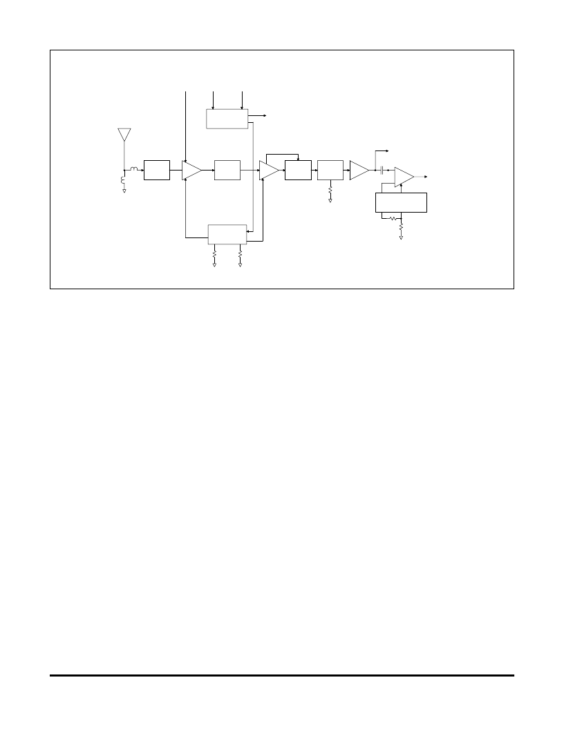
RX5500 ASH Receiver Block Diagram
Figure 2 is the general block diagram of the RX5500 ASH receiver.
Please refer to Figure 2 for the following discussions.
Antenna Port
The only external RF components needed for the receiver are the
antenna and its matching components. Antennas presenting an im-
pedance in the range of 35 to 72 ohms resistive can be satisfactorily
matched to the RFIO pin with a series matching coil and a shunt
matching/ESD protection coil. Other antenna impedances can be
matched using two or three components. For some impedances,
two inductors and a capacitor will be required. A DC path from RFIO
to ground is required for ESD protection.
Receiver Chain
The output of the SAW filter drives amplifier RFA1. The output of
RFA1 drives the SAW delay line, which has a nominal delay of
0.5 μs.
The second amplifier, RFA2, provides 51 dB of gain below satura-
tion. The output of RFA2 drives a full-wave detector with 19 dB of
threshold gain. The onset of saturation in each section of RFA2 is
detected and summed to provide a logarithmic response. This is
added to the output of the full-wave detector to produce an overall
detector response that is square law for low signal levels, and tran-
sitions into a log response for high signal levels. This combination
provides excellent threshold sensitivity and more than 70 dB of
detector dynamic range.
The detector output drives a gyrator filter. The filter provides a
three-pole, 0.05 degree equiripple low-pass response with excellent
group delay flatness and minimal pulse ringing. The 3 dB bandwidth
of the filter can be set from 4.5 kHz to 1.8 MHz with an external re-
sistor.
The filter is followed by a base-band amplifier which boosts the de-
tected signal to the BBOUT pin. When the receiver RF amplifiers
are operating at a 50%-50% duty cycle, the BBOUT signal changes
about 10 mV/dB, with a peak-to-peak signal level of up to 685 mV.
For lower duty cycles, the mV/dB slope and peak-to-peak signal
level are proportionately less. The detected signal is riding on a
1.1 Vdc level that varies somewhat with supply voltage, tempera-
ture, etc. BBOUT is coupled to the CMPIN pin or to an external data
recovery process (DSP, etc.) by a series capacitor. The correct
value of the series capacitor depends on data rate, data run length,
and other factors as discussed in the
ASH Transceiver Designer’s
Guide.
When the receiver is placed in the power-down (sleep) mode, the
output impedance of BBOUT becomes very high. This feature helps
preserve the charge on the coupling capacitor to minimize data
slicer stabilization time when the receiver switches out of the sleep
mode.
Data Slicer
The CMPIN pin drives data slicer DS1, which convert the analog
signal from BBOUT back into a digital stream. Data slicer DS1 is a
capacitively-coupled comparator with provisions for an adjustable
threshold. This threshold, or squelch, offsets the comparator’s slic-
ing level from 0 to 90 mV, and is set with a resistor between the
RREF and THLD1 pins. This threshold allows a trade-off between
receiver sensitivity and output noise density in the no-signal condi-
tion. For best sensitivity, the threshold is set to 0. In this case, noise
is output continuously when no signal is present. This, in turn, re-
quires the circuit being driven by the RXDATA pin to be able to pro-
cess noise (and signals) continuously.
This can be a problem if RXDATA is driving a circuit that must
“sleep” when data is not present to conserve power, or when it its
necessary to minimize false interrupts to a multitasking processor.
In this case, noise can be greatly reduced by increasing the thresh-
old level, but at the expense of sensitivity. The best 3 dB bandwidth
" # $
&
) * . / ( )
&
/ * ,
- 4
( ) ( (
&
5 - 6 )
)) 0- ,
- 2 3 + +
/ * ) ,
* + ) ) ( ) ,- ,
1
7
/ +
/ + - ( , - *
- 2 ) ,
- 2 (
- ( , - *
5 , ) + 5 - * 8
- ( , - *
&
) 9
5 * 8
#
$
!
%
!
"
:
/ (
/ ( "
/ (
/ (
/ ( %
:
:
:
:
: / ( $
:/ (
:
: / (
: / (
#
Figure 2
相關(guān)PDF資料 |
PDF描述 |
|---|---|
| RX5501 | Telecomm/Datacomm |
| RX5VL-E | 低功耗電壓檢測 |
| RX703000 | RD850 Task Debugger Windows(TM) based | User's Manual[06/2000] |
| RX703100 | RX850 Pro for Basics | User's Manual[04/2003] |
| RX730AE | FILTER NETZ EINBAU 6MH 250VAC 1A |
相關(guān)代理商/技術(shù)參數(shù) |
參數(shù)描述 |
|---|---|
| RX5501 | 功能描述:射頻接收器 2G ASH Receiver 315MHz 19.2kbps RoHS:否 制造商:Skyworks Solutions, Inc. 類型:GPS Receiver 封裝 / 箱體:QFN-24 工作頻率:4.092 MHz 工作電源電壓:3.3 V 封裝:Reel |
| RX-5502 | 制造商:Sherwood America 功能描述:Four Channel Stereo Receiver - 100W x 4 制造商:SHERWOOD 功能描述:STEREO RECEIVER 100W X 4 CHANNELS |
| RX550-TD256E | 制造商:Micro-Star International 功能描述:- Bulk |
| RX55257DPL | 制造商:TOSHIBA 制造商全稱:Toshiba Semiconductor 功能描述:MOS DIGITAL INTEGRATED CIRCUIT |
| RX-5567 | 功能描述:烙鐵 SOLDERING TIP RoHS:否 制造商:Weller 產(chǎn)品:Soldering Stations 類型:Digital, Iron, Stand, Cleaner 瓦特:50 W 最大溫度:+ 850 F 電纜類型:US Cord Included |
發(fā)布緊急采購,3分鐘左右您將得到回復(fù)。