- 您現(xiàn)在的位置:買賣IC網(wǎng) > PDF目錄382449 > RT9005BPSP (Richtek Technology Corporation) DDR VDDQ and Termination Voltage Regulator PDF資料下載
參數(shù)資料
| 型號: | RT9005BPSP |
| 廠商: | Richtek Technology Corporation |
| 英文描述: | DDR VDDQ and Termination Voltage Regulator |
| 中文描述: | 用于Vddq和終止電壓調(diào)節(jié)器 |
| 文件頁數(shù): | 8/10頁 |
| 文件大?。?/td> | 217K |
| 代理商: | RT9005BPSP |
RT9005A/B
Preliminary
8
DS9005A/B-01 September 2007
www.richtek.com
Application Information
Thermal Consideration
RT9005A/B regulators have internal thermal limiting
circuitry designed to protect the device during overload
conditions. For continued operation, do not exceed
maximum operation junction temperature 125
°
C. The
power dissipation definition in device is :
P
D
= (V
IN
- V
OUT
) x I
OUT
+ V
IN
x I
Q
The maximum power dissipation depends on the thermal
resistance of IC package, PCB layout, the rate of
surroundings airflow and temperature difference between
junction to ambient. The maximum power dissipation can
be calculated by following formula :
P
D(MAX)
= ( T
J(MAX)
-T
A
) /
θ
JA
Where T
J(MAX)
is the maximum operation junction
temperature 125
°
C, T
A
is the ambient temperature and
the
θ
JA
is the junction to ambient thermal resistance. The
junction to ambient thermal resistance (
θ
JA
is layout
dependent) for SOP-8 package (Exposed Pad) is 75
°
C/
W on standard JEDEC 51-7 (4 layers, 2S2P) thermal test
board. The maximum power dissipation at T
A
= 25
°
C can
be calculated by following formula :
P
D(MAX)
= (125
°
C - 25
°
C) / 75
°
C/W = 1.33W
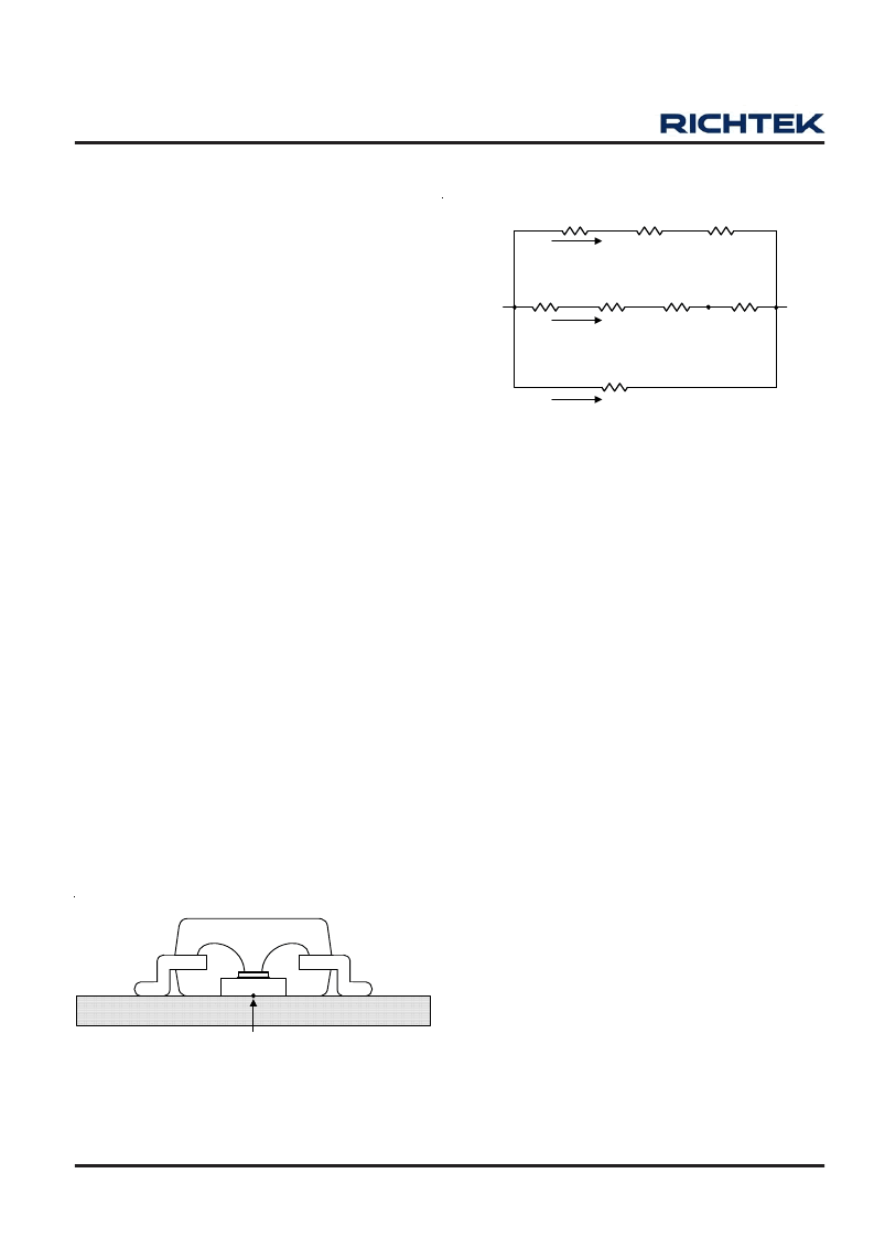
Figure 2 show the package sectional drawing of SOP-8
(Exposed Pad). Every package has several thermal
dissipation paths. As show in Figure 2, the thermal
resistance equivalent circuit of SOP-8 (Exposed Pad). The
path 2 is the main path due to these materials thermal
conductivity. We define the exposed pad is the case point
of the path 2.
Ambient
Molding Compound
Gold Line
Lead Frame
Die Pad
Case (Exposed Pad)
Figure 1. SOP-8 (Exposed Pad) Package Sectional
Drawing
Figure 2. Thermal Resistance Equivalent Circuit
Junction
R
DIE
R
DIE-ATTACH
R
DIE-PAD
R
GOLD-LINE
R
LEAD FRAME
Case
(Exposed Pad)
R
PCB
R
PCB
Ambient
R
MOLDING-COMPOUND
path 1
path 2
path 3
The thermal resistance
θ
JA
of SOP-8 (Exposed Pad) is
determined by the package design and the PCB design.
However, the package design has been decided. If
possible, it's useful to increase thermal performance by
the PCB design. The thermal resistance can be decreased
by adding copper under the expose pad of SOP-8
package.
About PCB layout
,
the Figure 3 show the relation between
thermal resistance
θ
JA
and copper area on a standard
JEDEC 51-7 (4 layers, 2S2P) thermal test board at
T
A
= 25
°
C.We have to consider the copper couldn't stretch
infinitely and avoid the tin overflow. We use the
“
dog-bone
”
copper patterns on the top layer as Figure 4.
As shown in Figure 5, the amount of copper area to which
the SOP-8 (Exposed Pad) is mounted affects thermal
performance. When mounted to the standard SOP-8
(Exposed Pad) pad of 2 oz. copper (Figure 5.a),
θ
JA
is
75
°
C/W. Adding copper area of pad under the SOP-8
(Exposed Pad) (Figure 5.b) reduces the
θ
JA
to 64
°
C/W.
Even further, increasing the copper area of pad to 70mm
2
(Figure 5.e) reduces the
θ
JA
to 49
°
C/W.
相關(guān)PDF資料 |
PDF描述 |
|---|---|
| RT9006A | Dual LDO Regulator with Reset Function |
| RT9006AGSP | Dual LDO Regulator with Reset Function |
| RT9006APSP | Dual LDO Regulator with Reset Function |
| RT9006BGSP | Dual LDO Regulator with Reset Function |
| RT9006BPSP | Dual LDO Regulator with Reset Function |
相關(guān)代理商/技術(shù)參數(shù) |
參數(shù)描述 |
|---|---|
| RT9006A | 制造商:RICHTEK 制造商全稱:Richtek Technology Corporation 功能描述:Dual LDO Regulator with Reset Function |
| RT9006AGSP | 制造商:RICHTEK 制造商全稱:Richtek Technology Corporation 功能描述:Dual LDO Regulator with Reset Function |
| RT9006APSP | 制造商:RICHTEK 制造商全稱:Richtek Technology Corporation 功能描述:Dual LDO Regulator with Reset Function |
| RT9006BGSP | 制造商:RICHTEK 制造商全稱:Richtek Technology Corporation 功能描述:Dual LDO Regulator with Reset Function |
| RT9006BPSP | 制造商:RICHTEK 制造商全稱:Richtek Technology Corporation 功能描述:Dual LDO Regulator with Reset Function |
發(fā)布緊急采購,3分鐘左右您將得到回復(fù)。