- 您現(xiàn)在的位置:買賣IC網(wǎng) > PDF目錄374597 > RM3182A (Fairchild Semiconductor Corporation) ARINC 429 Differential Line Driver(ARINC 429標(biāo)準(zhǔn)差分線驅(qū)動(dòng)器) PDF資料下載
參數(shù)資料
| 型號(hào): | RM3182A |
| 廠商: | Fairchild Semiconductor Corporation |
| 英文描述: | ARINC 429 Differential Line Driver(ARINC 429標(biāo)準(zhǔn)差分線驅(qū)動(dòng)器) |
| 中文描述: | ARINC公司429差分線路驅(qū)動(dòng)器(個(gè)ARINC 429標(biāo)準(zhǔn)差分線驅(qū)動(dòng)器) |
| 文件頁(yè)數(shù): | 2/12頁(yè) |
| 文件大小: | 66K |
| 代理商: | RM3182A |
RM3182A
PRODUCT SPECIFICATION
2
Functional Description
The device contains three main functional blocks. The first
block is a digital section used to decode the ARINC Clock,
Synchronization, and Data inputs as shown in Block Dia-
gram. This block takes these inputs and channels the data to
the charge pump circuits. The logical relationship for these
pins is presented in Table 1.
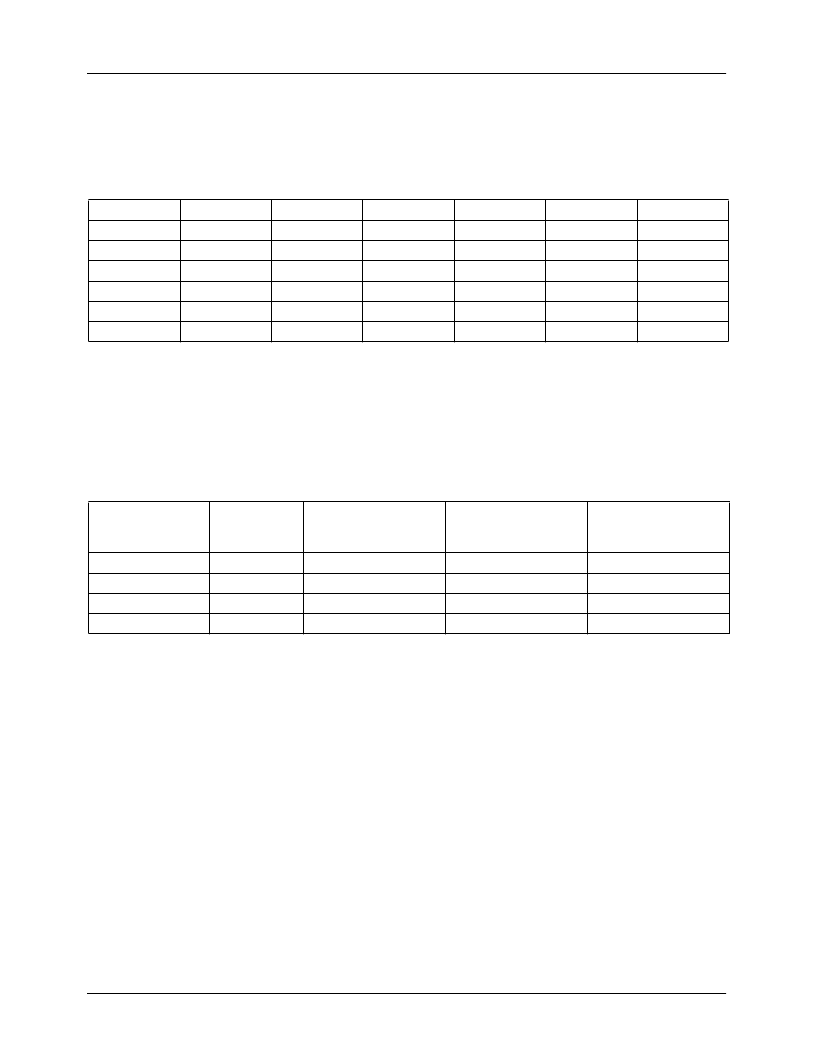
Table 1. I/O Truth Table
Sync
X
L
H
H
H
H
Clock
L
X
H
H
H
H
Data A
X
X
L
L
H
H
Data B
X
X
L
H
L
H
Out A
0V
0V
0V
-VREF
+VREF
0V
Out B
0V
0V
0V
+VREF
-VREF
0V
Comments
Null
Null
Null
Low
High
Null
The second functional block is a charge pump circuit that is
used to control the output waveform and its timing character-
istics. This is achieved through charging and discharging a
capacitor with a known current. The capacitor is user select-
able, and is connected between C
A rate select pin (digital input) enables to set the rise and fall
A
or C
B
pins and ground.
time. If this pin is tied to ground, the device functions in the
high rate. This mode is recommended if the user does not
have an application requiring data rate switching. In the table
below, recommended capacitor values are given for each
possible data combination.
Table 2. Rate Select Pin Truth Table
Rate Select
Logic 0
Logic 1
Logic 0
Logic 1
C
C
(pF)
56
56
390
390
A
B
10% to 90%
Rlse/Fall time
(
m
S)
1.5
10
10
N/A
Data Rate
(Kbits/sec)
100
12-14.5
12-14.5
N/A
Comments
High Rate
Low Rate
Low Rate
Not Used
The last functional block of the device consists of a voltage
follower and a high power output differential amplifier.
The voltage follower buffers the signals presented at the
charge caps and presents the mirrored signal to the differ-
ence
amplifier to drive the ARINC line. Two different outputs
are available from the differential amplifiers: Amp A, Amp
B, and Out A, Out B. The outputs Amp A and Amp B are the
direct outputs of the power amplifier. The outputs Out A and
Out B include 37.5
W
series resistors added to minimize bus
reflections by matching the power amplifier’s output imped-
ance to the cable’s impedance of 75
may be used to customize the output impedance of the
device. These outputs can also be used to enhance the
device’s drive capability. For example, driving the standard
30 nF || 400
W
load defined in the ARINC specifications (see
output drive capability and capacitive loads for more details).
All outputs are protected from voltage spikes with diodes
connected between the output pins and the supply lines.
W
. Amp A and Amp B
相關(guān)PDF資料 |
PDF描述 |
|---|---|
| RM3283 | Dual ARINC 429 Line Receiver |
| RM3283D | Dual ARINC 429 Line Receiver |
| RM35HG-34S | Super Fast Recovery Diodes |
| RM35HG-34S | Super Fast Recovery Single Diode (35 Amperes/1700 Volts) |
| RM400DY-66S | HIGH POWER, HIGH SPEED SWITCHING USE INSULATED TYPE |
相關(guān)代理商/技術(shù)參數(shù) |
參數(shù)描述 |
|---|---|
| RM3182AL | 制造商:未知廠家 制造商全稱:未知廠家 功能描述:Line Driver |
| RM3182AS | 制造商:未知廠家 制造商全稱:未知廠家 功能描述:Line Driver |
| RM3182L | 制造商:未知廠家 制造商全稱:未知廠家 功能描述:ARINC 429 Differential Line Driver |
| RM3182L/883B | 制造商:未知廠家 制造商全稱:未知廠家 功能描述:ARINC 429 Differential Line Driver |
| RM3182S | 制造商:未知廠家 制造商全稱:未知廠家 功能描述:ARINC 429 Differential Line Driver |
發(fā)布緊急采購(gòu),3分鐘左右您將得到回復(fù)。