- 您現(xiàn)在的位置:買賣IC網 > PDF目錄385769 > RF2637PCBA (RF Micro Devices, Inc.) RECEIVE AGC AMPLIFIER PDF資料下載
參數(shù)資料
| 型號: | RF2637PCBA |
| 廠商: | RF Micro Devices, Inc. |
| 英文描述: | RECEIVE AGC AMPLIFIER |
| 中文描述: | 接收AGC放大器 |
| 文件頁數(shù): | 2/8頁 |
| 文件大?。?/td> | 1021K |
| 代理商: | RF2637PCBA |
10-42
RF2637
Rev A3 040511
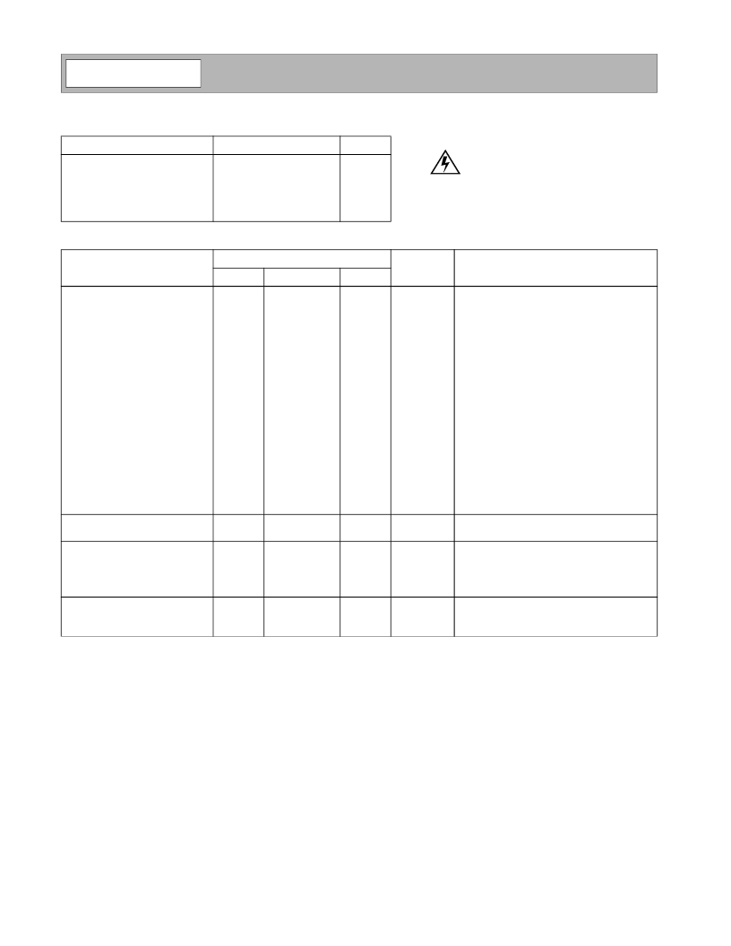
Absolute Maximum Ratings
Parameter
Supply Voltage
Control Voltage
Input RF Power
Operating Ambient Temperature
Storage Temperature
Value
-0.5 to +7.0
-0.5 to +5.0
+10
-40 to +85
-40 to +150
Unit
V
DC
V
DC
dBm
°C
°C
Parameter
Specification
Typ.
Unit
Condition
Min.
Max.
Overall
T=25°C, 85MHz, V
CC
=3.0V, Z
S
=500
,
Z
L
=500
, 500
External Input Terminating
Resistor, 500
External Output Terminating
Resistor (Effective Z
S
=333
, Effective
Z
L
=250
) (See Application Example)
Frequency Range
Maximum Gain
Minimum Gain
Maximum Gain
Minimum Gain
Gain Slope
Gain Control Voltage Range
Gain Control Input Impedance
Noise Figure
Input IP
3
12 to 385
+51
-55
+45
-58
57
0 to 2.5
30
5
-40
-2
MHz
dB
dB
dB
dB
dB/V
V
DC
k
dB
dBm
dBm
+40
-65
+35
-68
+65
-40
+55
-48
V
GC
=2.5V, 85MHz
V
GC
=0.1V, 85MHz
V
GC
=2.5V, 385MHz
V
GC
=0.1V, 385MHz
Note 1
Source impedance of 4.7k
7.2
At maximum gain and 85MHz
At +40dB gain, referenced to 500
At minimum gain, referenced to 500
Spurious<-70dBm
-46
Stability (Max VSWR)
IF Input
Input Impedance
Power Supply
Voltage
Current Consumption
10:1
1
k
CDMA, differential
2.7 to 3.4
10
11.5
V
6
7
15
15
mA
mA
Minimum gain, V
CC
=3.0V
Maximum gain, V
CC
=3.0V
Thermal
Thermal Resistance
Maximum Junction Temperature
Note 1: Measured between a gain control voltage of 1.0V to 1.5V.
150
90
°C/W
°C
Theta J-Ref 85°C
Ref 85°C
Caution!
ESD sensitive device.
RF Micro Devices believes the furnished information is correct and accurate
at the time of this printing. However, RF Micro Devices reserves the right to
make changes to its products without notice. RF Micro Devices does not
assume responsibility for the use of the described product(s).
相關PDF資料 |
PDF描述 |
|---|---|
| RF2705 | 887664300 |
| RF2705PCBA-41X | 887664400 |
| RF2713 | 887667300 |
| RF2721 | QUADRATURE DEMODULATOR |
| RF2909 | 3V 915MHZ SPREAD-SPECTRUM TRANSMITTER IC |
相關代理商/技術參數(shù) |
參數(shù)描述 |
|---|---|
| RF2637PCK-410 | 制造商:RF Micro Devices Inc 功能描述:KIT EVAL FOR RF2637 |
| RF2637TR7 | 制造商:RF Micro Devices Inc 功能描述:IC AGC AMP FOR 3V CELLULAR 8MSOP |
| RF2638 | 制造商:RFMD 制造商全稱:RF Micro Devices 功能描述:W-CDMA AND CDMA UPCONVERTER/ BPSK MODULATOR |
| RF2638_06 | 制造商:RFMD 制造商全稱:RF Micro Devices 功能描述:W-CDMA AND CDMA UPCONVERTER/ BPSK MODULATOR |
| RF2638-000 | 制造商:TE Connectivity 功能描述:FUSE 40A 72V RESETTABLE 2PIN - Tape and Reel 制造商:TE Connectivity 功能描述:RXEF090-2 |
發(fā)布緊急采購,3分鐘左右您將得到回復。