- 您現(xiàn)在的位置:買(mǎi)賣(mài)IC網(wǎng) > PDF目錄225034 > REF3333AIDCKT (TEXAS INSTRUMENTS INC) 1-OUTPUT THREE TERM VOLTAGE REFERENCE, 3.3 V, PDSO3 PDF資料下載
參數(shù)資料
| 型號(hào): | REF3333AIDCKT |
| 廠商: | TEXAS INSTRUMENTS INC |
| 元件分類(lèi): | 基準(zhǔn)電壓源/電流源 |
| 英文描述: | 1-OUTPUT THREE TERM VOLTAGE REFERENCE, 3.3 V, PDSO3 |
| 封裝: | GREEN, SC-70, 3 PIN |
| 文件頁(yè)數(shù): | 19/20頁(yè) |
| 文件大?。?/td> | 580K |
| 代理商: | REF3333AIDCKT |
第1頁(yè)第2頁(yè)第3頁(yè)第4頁(yè)第5頁(yè)第6頁(yè)第7頁(yè)第8頁(yè)第9頁(yè)第10頁(yè)第11頁(yè)第12頁(yè)第13頁(yè)第14頁(yè)第15頁(yè)第16頁(yè)第17頁(yè)第18頁(yè)當(dāng)前第19頁(yè)第20頁(yè)
www.ti.com
APPLICATIONS INFORMATION
SUPPLY VOLTAGE
START-UP TIME
V
IN
REF33xx
GND
V
OUT
1.2V
Bandgap
BASIC CONNECTIONS
REF33xx
V
IN
V
OUT
V
OUT
V
IN
C
BYPASS
1 Fto10 F
(recommended)
m
C
L
0.1 Fto10 F
m
GND
1V/div
Time(400 s/div)
m
V
IN
0.1 F
m
1 F
m
10 F
m
TEMPERATURE DRIFT
Drift=
V
-
OUTMAX
OUTMIN
V
TempRange
OUT
10 (ppm)
6
(1)
SBOS392A – AUGUST 2007 – REVISED SEPTEMBER 2007
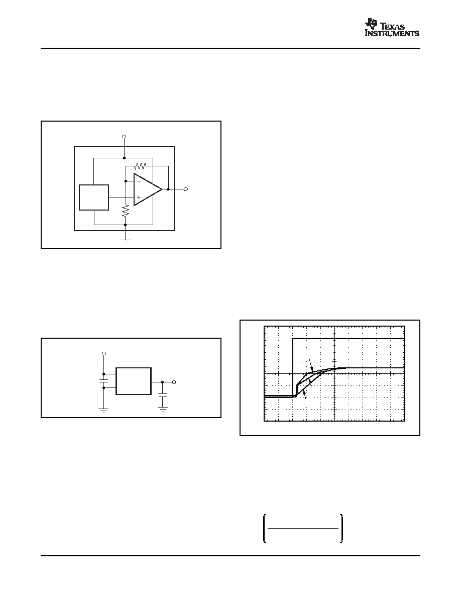
The REF33xx is a family of low-power, precision
bandgap voltage references that are specifically
The REF33xx family of voltage references features
designed for excellent initial voltage accuracy with a
extremely
low
dropout
voltage,
except
for
the
high output current. Figure 17 shows a simplified
REF3312. The REF3312 has a minimum supply
block diagram of the REF33xx.
requirement of 1.8V. These references can be
operated with a supply 110mV above the output
voltage with a 5mA load (typical). For loaded
conditions, a typical dropout voltage versus load
graph is illustrated in Figure 4 of the Typical
Characteristics.
If the supply voltage connected to the IN pin is rapidly
moved while the
REF33xx
is
connected
to
a
capacitive load, a reverse voltage may discharge
through the OUT pin and into the REF33xx device.
This voltage will not damage the REF33xx, provided
that it is less than or equal to 5V.
The REF33xx features an advanced start-up circuit.
Start-up time is almost independent of load (with a
Figure 17. REF33xx Simplified Block Diagram
0.1
μF to 10μF load). Upon start-up, the current boost
circuit forces the output voltage. When the preset
voltage is reached, the REF33xx switches to the
second stage of output circuitry to precisely set the
output voltage. Figure 19 shows the start-up time of
the REF3325 for three different capacitive loads. In
REF33xx. A recommended supply bypass capacitor
all three cases, the output voltage settles within 2ms.
ranging between 1
μF to 10μF is recommended. The
total capacitive load at the output must be between
0.1
μF to 10μF to ensure output stability.
Figure 18. Basic Connections
Figure 19. Start-Up Time
The REF33xx is designed for minimal drift error,
defined as the change in output voltage over
temperature. The drift is calculated using the box
method, as described in Equation 1:
8
Copyright 2007, Texas Instruments Incorporated
相關(guān)PDF資料 |
PDF描述 |
|---|---|
| REF5045IDGKT | 1-OUTPUT THREE TERM VOLTAGE REFERENCE, 4.5 V, PDSO8 |
| REG101NA-2.5/250G4 | 2.5 V FIXED POSITIVE LDO REGULATOR, 0.13 V DROPOUT, PDSO5 |
| REG101NA-2.5/3KG4 | 2.5 V FIXED POSITIVE LDO REGULATOR, 0.13 V DROPOUT, PDSO5 |
| REG101NA-2.8/250G4 | 2.8 V FIXED POSITIVE LDO REGULATOR, 0.13 V DROPOUT, PDSO5 |
| REG101UA-2.5G4 | 2.5 V FIXED POSITIVE LDO REGULATOR, 0.13 V DROPOUT, PDSO8 |
相關(guān)代理商/技術(shù)參數(shù) |
參數(shù)描述 |
|---|---|
| REF3333AIDCKTG4 | 功能描述:基準(zhǔn)電壓& 基準(zhǔn)電流 30ppm/C Drift 3.9uA Vltg Ref RoHS:否 制造商:STMicroelectronics 產(chǎn)品:Voltage References 拓?fù)浣Y(jié)構(gòu):Shunt References 參考類(lèi)型:Programmable 輸出電壓:1.24 V to 18 V 初始準(zhǔn)確度:0.25 % 平均溫度系數(shù)(典型值):100 PPM / C 串聯(lián) VREF - 輸入電壓(最大值): 串聯(lián) VREF - 輸入電壓(最小值): 分流電流(最大值):60 mA 最大工作溫度:+ 125 C 封裝 / 箱體:SOT-23-3L 封裝:Reel |
| REF3425IDBVR | 功能描述:REF3425 - 20 PPM/C IQ 85UA 制造商:texas instruments 系列:* 包裝:剪切帶(CT) 零件狀態(tài):在售 安裝類(lèi)型:表面貼裝 封裝/外殼:SOT-23-6 供應(yīng)商器件封裝:SOT-23-6 標(biāo)準(zhǔn)包裝:1 |
| REF401 | 制造商:General Tools 功能描述:GLYCOL REFRACTOMETER TO MEASURE FREEZING POINT (-60 TO 32 F) |
| REF43 | 制造商:AD 制造商全稱(chēng):Analog Devices 功能描述:+2.5V Low Power Precision Voltage Reference |
| REF-43 | 制造商:AD 制造商全稱(chēng):Analog Devices 功能描述:+2.5V Low Power Precision Voltage Reference |
發(fā)布緊急采購(gòu),3分鐘左右您將得到回復(fù)。