- 您現(xiàn)在的位置:買賣IC網(wǎng) > PDF目錄372040 > RD-19230FX-203 Resolver-to-Digital Converter PDF資料下載
參數(shù)資料
| 型號(hào): | RD-19230FX-203 |
| 元件分類: | ADC |
| 英文描述: | Resolver-to-Digital Converter |
| 中文描述: | 分解器數(shù)字轉(zhuǎn)換器 |
| 文件頁(yè)數(shù): | 12/20頁(yè) |
| 文件大?。?/td> | 152K |
| 代理商: | RD-19230FX-203 |
第1頁(yè)第2頁(yè)第3頁(yè)第4頁(yè)第5頁(yè)第6頁(yè)第7頁(yè)第8頁(yè)第9頁(yè)第10頁(yè)第11頁(yè)當(dāng)前第12頁(yè)第13頁(yè)第14頁(yè)第15頁(yè)第16頁(yè)第17頁(yè)第18頁(yè)第19頁(yè)第20頁(yè)
12
Data Device Corporation
www.ddc-web.com
RD-19230
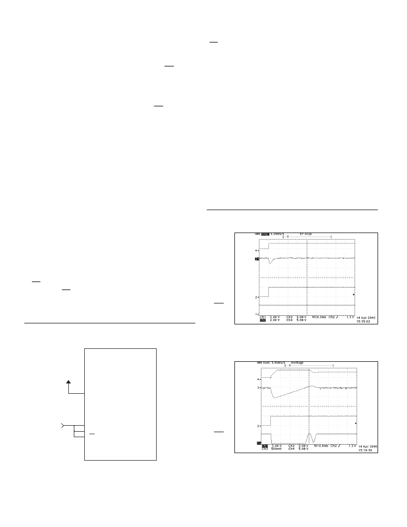
FIGURE 17. BENEFIT OF SWITCHING
RESOLUTION ON THE FLY
Without Switch Resolution on the Fly Implemented
VEL
ERROR
D0
BIT
0V
-5V
0V
0V
5V
5V
0
°
ERROR = 1500 LSBs per box
When this system uses the switch resolution on the fly imple-
mentation, the velocity signal immediately assumes the pre-
charged level of the second set of components, resulting in small
errors and reduced settling times. Notice that the BIT output,
in FIGURE 17, does not indicate a fault condition.
When this system type does not use the switch resolution on the
fly implementation, large errors and increased settling times
result. The errors exceed 100 LSBs causing the BIT to flag for a
fault condition.
SWITCH ON THE FLY IMPLEMENTATION
The following steps detail switching resolution on the fly.
1) The SHIFT pin should be controlled synchronously with the
change in resolution. When shift is logic high, the VEL1 compo-
nents will be selected. When shift is logic 0, the VEL2 compo-
nents will be selected.
2) The second set of BW components (C
BW2
, R
B2
, C
BW2/10
)
should typically be of the same value as the first set (C
BW1
, R
B1
,
C
BW1/10
,) and should be installed on VEL
2
and VEL SJ
2
.
Note: Each set of bandwidth components must be chosen to
insure that the tracking rate to BW ratio (listed in TABLE 2,
on page 4) is not exceeded for the resolution in which it will
be used.
3) UP/DN will program the direction of the gain. If the resolution
is increasing (UP/DN logic 0), the gain of the pre-charge amplifi-
er should be set to four.
If the resolution is decreasing
With Switch Resolution on the Fly Implemented
VEL
ERROR
D0
BIT
0V
-5V
0V
0V
5V
5V
0
°
ERROR = 13.6 LSBs per box
27
58
+5V
UP/DN
SHIFT
RD-19230
D1
D0
FIGURE 16. INPUT WIRING - SWITCHING ON THE FLY
BETWEEN 14 AND 16 BIT RESOLUTION
(UP/DN logic 1), the gain should be set to 1/4. The gain of the
pre-charge amplifier should be programmed prior to switching
the resolution of the converter, allowing enough time for the com-
ponents to settle to the pre-charged level. This time will depend
on the time constant of the bandwidth components being
charged. If switching is limited to two adjacent resolutions (i.e.,
14 and 16) then the pre-charge amplifier can be set up to con-
tinuously maintain the appropriate velocity voltage on the dese-
lected components, resulting in the fastest possible switching
times. See FIGURE 16 for an example of the input wiring con-
nections necessary for switching on the fly between 14 and 16
bit resolution.
DUAL BANDWIDTHS
With the second set of BW component pins, the user can set two
bandwidths for the RD-19230 and choose between them.To use
two bandwidths, proceed as follows:
相關(guān)PDF資料 |
PDF描述 |
|---|---|
| RD-19230FX-203T | Resolver-to-Digital Converter |
| RD-19230FX-302 | Resolver-to-Digital Converter |
| RD30HVF1 | TRANSISTOR | MOSFET | N-CHANNEL | 30V V(BR)DSS | SOT-391VAR |
| RD6610ANP-011 | Analog Shift Register |
| RE003B | DC-to-DC Voltage Converter |
相關(guān)代理商/技術(shù)參數(shù) |
參數(shù)描述 |
|---|---|
| RD-19230FX-203T | 制造商:未知廠家 制造商全稱:未知廠家 功能描述:RESOLVER-TO-DIGITAL CONVERTER |
| RD-19230FX-302 | 制造商:未知廠家 制造商全稱:未知廠家 功能描述:Resolver-to-Digital Converter |
| RD-19230FX-302T | 制造商:未知廠家 制造商全稱:未知廠家 功能描述:Resolver-to-Digital Converter |
| RD-19230FX-303 | 制造商:未知廠家 制造商全稱:未知廠家 功能描述:Resolver-to-Digital Converter |
| RD-19230FX-303T | 制造商:未知廠家 制造商全稱:未知廠家 功能描述:Resolver-to-Digital Converter |
發(fā)布緊急采購(gòu),3分鐘左右您將得到回復(fù)。