- 您現(xiàn)在的位置:買(mǎi)賣(mài)IC網(wǎng) > PDF目錄299830 > R1150H007C-T1 (RICOH COMPANY LTD) 3.5 V FIXED POSITIVE LDO REGULATOR, 0.35 V DROPOUT, PDSO5 PDF資料下載
參數(shù)資料
| 型號(hào): | R1150H007C-T1 |
| 廠商: | RICOH COMPANY LTD |
| 元件分類: | 固定正電壓?jiǎn)温份敵鯨DO穩(wěn)壓器 |
| 英文描述: | 3.5 V FIXED POSITIVE LDO REGULATOR, 0.35 V DROPOUT, PDSO5 |
| 封裝: | LEAD FREE, SOT-89, 5 PIN |
| 文件頁(yè)數(shù): | 26/30頁(yè) |
| 文件大小: | 338K |
| 代理商: | R1150H007C-T1 |
第1頁(yè)第2頁(yè)第3頁(yè)第4頁(yè)第5頁(yè)第6頁(yè)第7頁(yè)第8頁(yè)第9頁(yè)第10頁(yè)第11頁(yè)第12頁(yè)第13頁(yè)第14頁(yè)第15頁(yè)第16頁(yè)第17頁(yè)第18頁(yè)第19頁(yè)第20頁(yè)第21頁(yè)第22頁(yè)第23頁(yè)第24頁(yè)第25頁(yè)當(dāng)前第26頁(yè)第27頁(yè)第28頁(yè)第29頁(yè)第30頁(yè)
R1150H
5
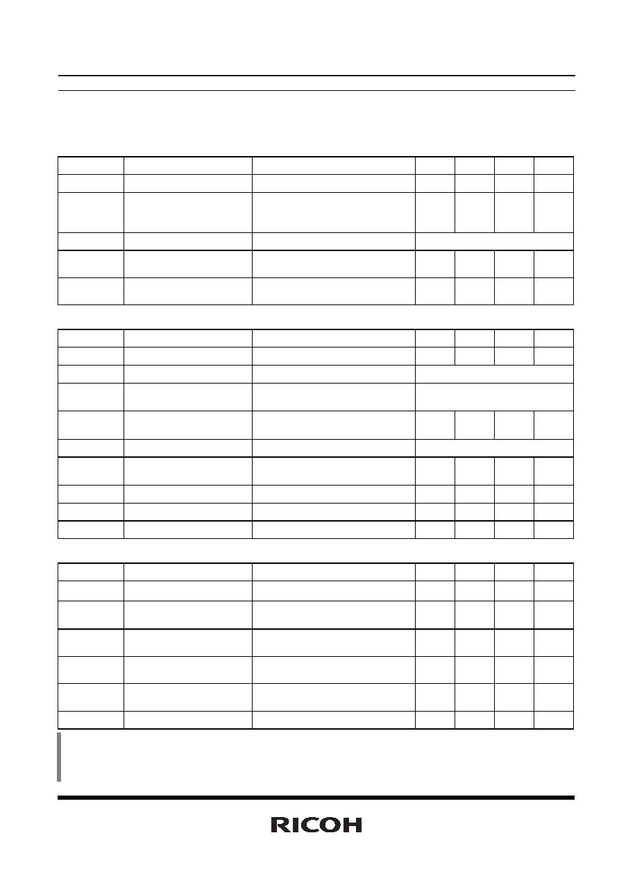
ELECTRICAL CHARACTERISTICS
R1150HxxxA
Topt
=25°C
Symbol
Item
Conditions
Min.
Typ.
Max.
Unit
VIN
Input Voltage
24.0
V
ISS
Supply Current
VIN=VCE
VOUT
≥ (-VDET): VIN=VOUT+2.0V
VOUT < (-VDET): VIN=(-VDET)+2.0V
7
14
μA
Istandby
Standby Current
VDD=24V, VCE=0V
Refer to Supply Current Table
TTSD
Thermal Shutdown
Temperature
Junction Temperature
150
°C
TTSR
Thermal Shutdown
Released Temperature
Junction Temperature
120
°C
VR
Topt
=25°C
Symbol
Item
Conditions
Min.
Typ.
Max.
Unit
VOUT
Output Voltage
VIN=VOUT+2.0V, IOUT=20mA
×0.98
×1.02
V
IOUT1
Output Current
VIN=VOUT+2.0V
Refer to Output Current Table
ΔVOUT/ΔIOUT Load Regulation
VIN=VOUT+2.0V
1mA
≤ IOUT ≤ 40mA
Refer to Load Regulation Table
ΔVOUT/ΔVIN
Line Regulation
VIN=VOUT+2.0V, IOUT=20 mA
VOUT+1V
≤ VIN ≤ 24V
0.05
0.15
%/V
VDIF
Dropout Voltage
IOUT=20mA
Refer to Dropout Voltage Table
ΔVOUT/ΔTopt
Output Voltage
Temperature Coefficient
VIN=VOUT+2.0V, IOUT=20mA
40°C ≤ Topt ≤ 85°C
±100
ppm/°C
Ilim
Short Current Limit
VOUT=0V
45
mA
VCEH
CE "H" Input Voltage
1.5
VIN
V
VCEL
CE "L" Input Voltage
0
0.25
V
VD
Topt
=25°C
Symbol
Item
Conditions
Min.
Typ.
Max.
Unit
-VDET
×0.975
×1.025
V
VHYS
Detector Threshold
Hysteresis
-VDET
×0.03
-VDET
×0.05
-VDET
×0.07
V
IOUT2
Output Current
(Driver Output Pin)
Refer to Test Conditions for
Output Current Table
0.17
mA
VDDL
Minimum Operating
Voltage
*Note 1
0.9
1.2
V
Δ-VDET/ΔTopt
Detector Threshold
Temperature Coefficient
40°C ≤ Topt ≤ 85°C
±100
ppm/°C
tPLH
Output Delay Time
*Note 2
0.5
1.0
ms
Note 1) This item means VDD Voltage when Output Voltage is equal or less than 0.1V.
(Pull-up Resistor=470kW, Pull up Voltage=5V)
Note 2) VDET pin is pulled up to VDD via 470kW. tPLH means time interval from rising edge of VDD from
(-VDET)
2.0V to (-VDET)+2.0V to the point of Output Voltage being 80% of pull-up voltage.
相關(guān)PDF資料 |
PDF描述 |
|---|---|
| R1150H009C-T1 | 5 V FIXED POSITIVE LDO REGULATOR, 0.35 V DROPOUT, PDSO5 |
| R1150H010A-T1 | 3 V FIXED POSITIVE LDO REGULATOR, 0.4 V DROPOUT, PDSO5 |
| R1150H011A-T1 | 7 V FIXED POSITIVE LDO REGULATOR, 0.35 V DROPOUT, PDSO5 |
| R1150H014A-T1 | 7.5 V FIXED POSITIVE LDO REGULATOR, 0.45 V DROPOUT, PDSO5 |
| R1150H015A-T1 | 3 V FIXED POSITIVE LDO REGULATOR, 0.4 V DROPOUT, PDSO5 |
相關(guān)代理商/技術(shù)參數(shù) |
參數(shù)描述 |
|---|---|
| R1150HXXXX | 制造商:未知廠家 制造商全稱:未知廠家 功能描述:Power Management ICs |
| R1151 | 制造商:Rochester Electronics LLC 功能描述: |
| R11-51-.500A-B107EV-S | 制造商:Sensata Technologies 功能描述:R11-51-.500A-B107EV-S /Pole # 1 /Prod Family: 0213 |
| R11-51-.500A-G107EV | 制造商:Sensata Technologies 功能描述:Circuit Breaker Magnetic Circuit Protectors 1Pole 0.5A |
| R11-51-1.00A-W124EV | 制造商:Sensata Technologies 功能描述:Circuit Breaker Magnetic Circuit Protectors 1Pole 1A |
發(fā)布緊急采購(gòu),3分鐘左右您將得到回復(fù)。