- 您現(xiàn)在的位置:買賣IC網(wǎng) > PDF目錄382397 > PTPM749A (NXP SEMICONDUCTORS) Microcontroller with TrackPoint microcode from IBM PDF資料下載
參數(shù)資料
| 型號: | PTPM749A |
| 廠商: | NXP SEMICONDUCTORS |
| 元件分類: | 微控制器/微處理器 |
| 英文描述: | Microcontroller with TrackPoint microcode from IBM |
| 中文描述: | 8-BIT, MROM, MICROCONTROLLER, PQCC28 |
| 文件頁數(shù): | 8/14頁 |
| 文件大小: | 100K |
| 代理商: | PTPM749A |

Philips Semiconductors
Product specification
TPM749
Microcontroller with TrackPoint
microcode from IBM
1996 May 01
8
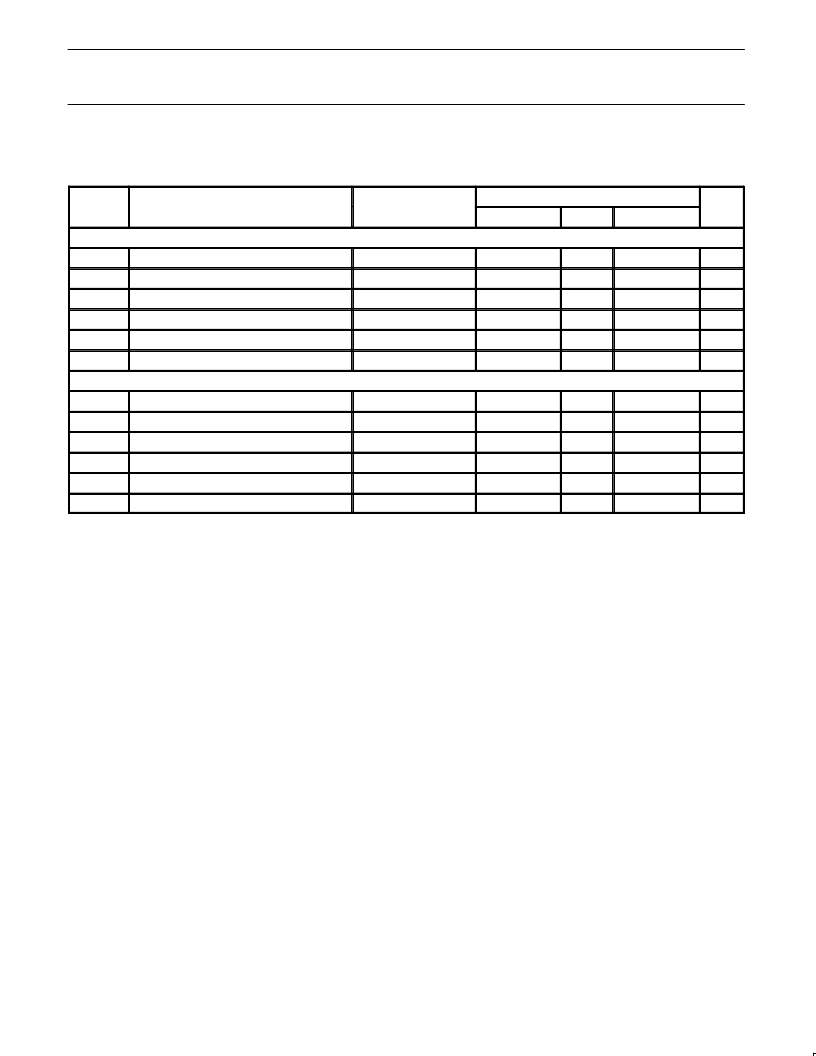
DC ELECTRICAL CHARACTERISTICS
(Continued)
T
amb
= 0
°
C to +70
°
C, AV
CC
= 5V
±
5, AV
SS
= 0V
4
V
CC
= 5V
±
10%, V
SS
= 0V
TEST
LIMITS
4
SYMBOL
PARAMETER
CONDITIONS
MIN
TYP
1
MAX
UNIT
Analog Inputs
(A/D guaranteed only with quartz window covered.)
AV
CC
Analog supply voltage
10
AV
CC
= V
CC
±
0.2V
4.5
5.5
V
AI
CC
Analog operating supply current
AV
CC
= 5.12V
3
9
mA
AV
IN
Analog input voltage
AV
SS
–0.2
AV
CC
+0.2
V
C
IA
Analog input capacitance
15
pF
t
ADS
Sampling time
8t
CY
s
t
ADC
Conversion time
40t
CY
s
Analog Inputs
(A/D guaranteed only with quartz window covered.) (Continued)
R
Resolution
8
bits
E
RA
Relative accuracy
±
1
LSB
OS
e
Zero scale offset
±
1
LSB
G
e
Full scale gain error
0.4
%
M
CTC
Channel to channel matching
±
1
LSB
C
t
Crosstalk
0–100kHz
–60
dB
NOTES:
1. Stresses above those listed under Absolute Maximum Ratings may cause permanent damage to the device. This is a stress rating only and
functional operation of the device at these or any conditions other than those described in the AC and DC Electrical Characteristics section
of this specification is not implied.
2. Under steady state (non-transient) conditions, I
OL
must be externally limited as follows:
Maximum I
OL
per port pin:
10mA
Maximum I
OL
per 8-bit port:
26mA
Maximum total I
OL
for all outputs:
67mA
If I
OL
exceeds the test condition, V
OL
may exceed the related specification. Pins are not guaranteed to sink current greater than the listed
test conditions.
3. This product includes circuitry specifically designed for the protection of its internal devices from the damaging effects of excessive static
charge. Nonetheless, it is suggested that conventional precautions be taken to avoid applying greater than the rated maxima.
4. Parameters are valid over operating temperature range unless otherwise specified. All voltages are with respect to V
SS
unless otherwise
noted.
5. Power-down I
is measured with all output pins disconnected; port 0 = V
CC
; X2, X1 n.c.; RST = V
.
6. I
is measured with all output pins disconnected; X1 driven with t
, t
CHCL
= 5ns, V
IL
= V
SS
+ 0.5V, V
IH
= V
CC
– 0.5V; X2 n.c.;
RST = port 0 = V
. I
will be slightly higher if a crystal oscillator is used.
7. Idle I
is measured with all output pins disconnected; X1 driven with t
CLCH
, t
CHCL
= 5ns, V
IL
= V
SS
+ 0.5V, V
IH
= V
CC
– 0.5V; X2 n.c.;
port 0 = V
CC;
RST = V
SS
.
8. Load capacitance for ports = 80pF.
9. The resistor ladder network is not disconnected in the power down or idle modes. Thus, to conserve power, the user may remove AV
CC
.
10.If the A/D function is not required, or if the A/D function is only needed periodically, AV
CC
may be removed without affecting the operation of
the digital circuitry. Contents of ADCON and ADAT are not guaranteed to be valid. If AV
CC
is removed, the A/D inputs must be lowered to
less than 0.5V. Digital inputs on P1.0–P1.4 will not function normally.
11. These parameters do not apply to P1.0–P1.4 if the A/D function is enabled.
相關PDF資料 |
PDF描述 |
|---|---|
| PTPM749DB | Microcontroller with TrackPoint microcode from IBM |
| PTPM754ADB | Microcontroller with TrackPoint microcode from IBM |
| PTT-1616 | MODEM TRANSFORMER |
| PTT-1617 | MODEM TRANSFORMER |
| PTT-1618 | MODEM TRANSFORMER |
相關代理商/技術參數(shù) |
參數(shù)描述 |
|---|---|
| PTPM749DB | 制造商:PHILIPS 制造商全稱:NXP Semiconductors 功能描述:Microcontroller with TrackPoint microcode from IBM |
| PTPM754ADB | 制造商:PHILIPS 制造商全稱:NXP Semiconductors 功能描述:Microcontroller with TrackPoint microcode from IBM |
| PTPM754DB | 制造商:NXP Semiconductors 功能描述: |
| PTPS630WHI | 制造商:Siemens 功能描述:Wht 1pillar MK pinnacle trunking,630mm L |
| PTPS65800RTQR | 制造商:Texas Instruments 功能描述: |
發(fā)布緊急采購,3分鐘左右您將得到回復。