- 您現(xiàn)在的位置:買賣IC網(wǎng) > PDF目錄98065 > PTH12040WAD (TEXAS INSTRUMENTS INC) 1-OUTPUT DC-DC REG PWR SUPPLY MODULE PDF資料下載
參數(shù)資料
| 型號(hào): | PTH12040WAD |
| 廠商: | TEXAS INSTRUMENTS INC |
| 元件分類: | 電源模塊 |
| 英文描述: | 1-OUTPUT DC-DC REG PWR SUPPLY MODULE |
| 封裝: | ROHS COMPLIANT, DIP-20 |
| 文件頁數(shù): | 21/27頁 |
| 文件大小: | 633K |
| 代理商: | PTH12040WAD |
第1頁第2頁第3頁第4頁第5頁第6頁第7頁第8頁第9頁第10頁第11頁第12頁第13頁第14頁第15頁第16頁第17頁第18頁第19頁第20頁當(dāng)前第21頁第22頁第23頁第24頁第25頁第26頁第27頁
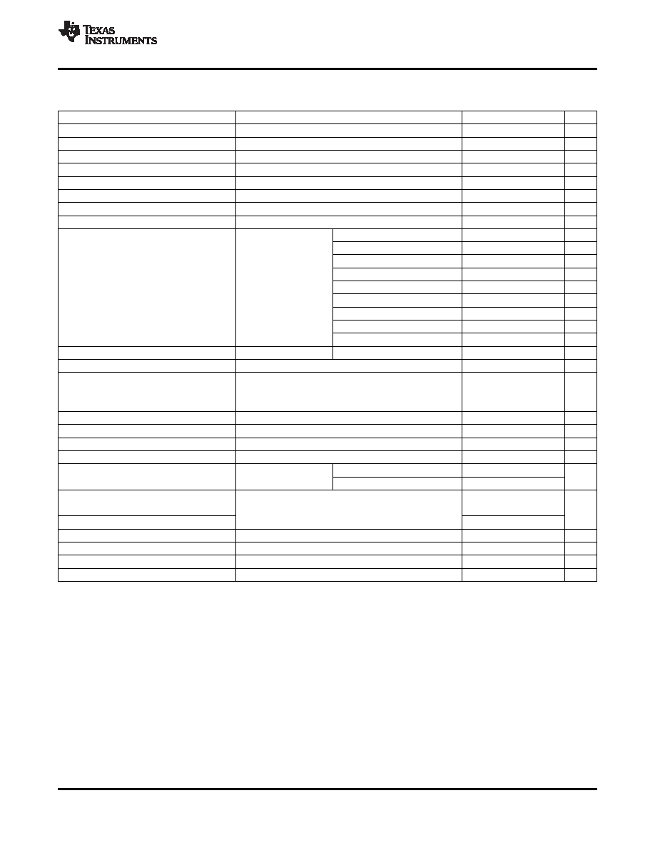
ELECTRICAL CHARACTERISTICS
www.ti.com............................................................................................................................................... SLTS237G – DECEMBER 2004 – REVISED MARCH 2009
TA = 25°C, VI = 12 V, VO = 3.3 V, CI = 1000 F, CO = 660 F, and IO = IOmax (unless otherwise stated)
PARAMETER
TEST CONDITIONS
MIN
TYP
MAX
UNIT
IO
Output current
60°C, 200 LFM airflow
0
50(1)
A
VI
Input voltage range
Over IO range
8(2)
14
V
VOtol
Set-point voltage tolerance
±2(3)
%VO
ΔRegtemp
Temperature variation
–40°C < TA < 85°C
±0.5
%VO
ΔRegline
Line regulation
Over VI range
±5
mV
ΔRegload
Load regulation
Over IO range
±5
mV
ΔRegtot
Total output variation
Includes set-point, line, load, –40°C
≤ TA ≤ 85°C
±3(3)
%VO
ΔRegadj
Output adjust range
0.8
5.5(2)
V
RSET = 205 , VO = 5.0 V
96%
RSET = 1.5 k, VO = 3.3 V
95%
RSET = 3.01 k, VO = 2.5 V
93%
RSET = 4.99 k, VO = 2.0 V
92%
η
Efficiency
IO = 35 A
RSET = 6.34 k, VO = 1.8 V
91%
RSET = 9.76 k, VO = 1.5 V
90%
RSET = 18.2 k, VO = 1.2 V
88%
RSET = 38.3 k, VO = 1.0 V
86%
RSET = open circuit, VO = 0.8 V
82%
VR
VO ripple (pk-pk)
20 MHz bandwidth
All voltages
15
mVpp
IOtrip
Overcurrent threshold
Reset, followed by auto-recovery
95
A
Transient response
1 A/s load step, 50 to 100% IOmax, CO = 660 F
trr
Recovery time
70
Sec
ΔVtr
VO over/undershoot
150
mV
VOadj
Margin up/down adjust
With Margin up/down control
±5%
IILmargin
Margin input current
Pin to GND
–8(4)
A
IILtrack
Track input current (pin 18)
Pin to GND
–0.10(5)
mA
dVtrack/dt
Track slew rate capability
|VTRACK – VO | ≤ 50 mV and VTRACK < VO(nom)
1
V/ms
UVLO
Undervoltage lockout
Pin 8 open
On-threshold
7.5(6)
V
Hysterisis
1(6)
Inhibit control (pin 7)
Referenced to GND
VIH
Input high voltage
2.5
Open(7)
V
VIL
Input low voltage
–0.2
0.5
IILinhibit
Input low current
Pin to GND
0.5
mA
IIinh
Input standby current
Inhibit (pin 7) to GND
35
mA
f s
Switching frequency
Over VI and IO ranges
0.9
1.05
1.2
MHz
CI
External input capacitance
560(8)
1000
F
(1)
See SOA curves or consult factory for appropriate derating.
(2)
When the set-point voltage is adjusted higher than 3.6 V, a 10-V minimum input voltage is recommended.
(3)
The set-point voltage tolerance is affected by the tolerance of RSET. The stated limit is unconditionally met if RSET has a tolerance of 1%
with 100 ppm/°C or better temperature stability.
(4)
A small, low-leakage (<100 nA) MOSFET is recommended to control this pin. The open-circuit voltage is less than 1 Vdc.
(5)
This control pin has an internal pull-up to 6.7 V. If left open-circuit, the module operates when input power is applied. A small, low
leakage (<100 nA) MOSFET or open-drain/collector voltage supervisor IC is recommended for control. See the Application Information
section for further guidance.
(6)
Default voltages may be adjusted using the UVLO Prog control input. See the Application Information section for further guidance.
(7)
This control pin has an internal pull-up to 5 V nominal. If it is left open-circuit, the module operates when input power is applied. A small,
low-leakage (<100 nA) MOSFET is recommended for control. Do not place an external pull-up on this pin. For further information, see
the related application note.
(8)
A minimum capacitance of 560-F is required at the input for proper operation. For best results, 1000 F is recommended. The
capacitance must be rated for a minimum of 300 mArms of ripple current.
Copyright 2004–2009, Texas Instruments Incorporated
3
Product Folder Link(s): PTH12040W
相關(guān)PDF資料 |
PDF描述 |
|---|---|
| PTH12040WAST | 1-OUTPUT DC-DC REG PWR SUPPLY MODULE |
| PTH12040WAH | 1-OUTPUT DC-DC REG PWR SUPPLY MODULE |
| PTH12040WAZ | 1-OUTPUT DC-DC REG PWR SUPPLY MODULE |
| PTN04050AAST | 1 A SWITCHING REGULATOR, 310 kHz SWITCHING FREQ-MAX, PDMA5 |
| PTN04050AAD | 1 A SWITCHING REGULATOR, 310 kHz SWITCHING FREQ-MAX, PDMA5 |
相關(guān)代理商/技術(shù)參數(shù) |
參數(shù)描述 |
|---|---|
| PTH12040WADT | 制造商:ARTESYN 制造商全稱:Artesyn Technologies 功能描述:DC-DC CONVERTERS POLA Non-isolated |
| PTH12040WAH | 功能描述:DC/DC轉(zhuǎn)換器 50-A 8-14V-Inp Wide Out Adj Pwr Module RoHS:否 制造商:Murata 產(chǎn)品: 輸出功率: 輸入電壓范圍:3.6 V to 5.5 V 輸入電壓(標(biāo)稱): 輸出端數(shù)量:1 輸出電壓(通道 1):3.3 V 輸出電流(通道 1):600 mA 輸出電壓(通道 2): 輸出電流(通道 2): 安裝風(fēng)格:SMD/SMT 封裝 / 箱體尺寸: |
| PTH12040WAHT | 制造商:ARTESYN 制造商全稱:Artesyn Technologies 功能描述:DC-DC CONVERTERS POLA Non-isolated |
| PTH12040WAS | 功能描述:DC/DC轉(zhuǎn)換器 50-A 8-14V-Inp Wide Out Adj Pwr Module RoHS:否 制造商:Murata 產(chǎn)品: 輸出功率: 輸入電壓范圍:3.6 V to 5.5 V 輸入電壓(標(biāo)稱): 輸出端數(shù)量:1 輸出電壓(通道 1):3.3 V 輸出電流(通道 1):600 mA 輸出電壓(通道 2): 輸出電流(通道 2): 安裝風(fēng)格:SMD/SMT 封裝 / 箱體尺寸: |
| PTH12040WAST | 功能描述:DC/DC轉(zhuǎn)換器 50A,8-14Vin,Wide- Out Adj Pwr Mod RoHS:否 制造商:Murata 產(chǎn)品: 輸出功率: 輸入電壓范圍:3.6 V to 5.5 V 輸入電壓(標(biāo)稱): 輸出端數(shù)量:1 輸出電壓(通道 1):3.3 V 輸出電流(通道 1):600 mA 輸出電壓(通道 2): 輸出電流(通道 2): 安裝風(fēng)格:SMD/SMT 封裝 / 箱體尺寸: |
發(fā)布緊急采購,3分鐘左右您將得到回復(fù)。