- 您現(xiàn)在的位置:買(mǎi)賣(mài)IC網(wǎng) > PDF目錄98065 > PTH12030WAZT (TEXAS INSTRUMENTS INC) 1-OUTPUT DC-DC REG PWR SUPPLY MODULE PDF資料下載
參數(shù)資料
| 型號(hào): | PTH12030WAZT |
| 廠商: | TEXAS INSTRUMENTS INC |
| 元件分類(lèi): | 電源模塊 |
| 英文描述: | 1-OUTPUT DC-DC REG PWR SUPPLY MODULE |
| 封裝: | ROHS COMPLIANT PACKAGE-13 |
| 文件頁(yè)數(shù): | 6/26頁(yè) |
| 文件大?。?/td> | 794K |
| 代理商: | PTH12030WAZT |
第1頁(yè)第2頁(yè)第3頁(yè)第4頁(yè)第5頁(yè)當(dāng)前第6頁(yè)第7頁(yè)第8頁(yè)第9頁(yè)第10頁(yè)第11頁(yè)第12頁(yè)第13頁(yè)第14頁(yè)第15頁(yè)第16頁(yè)第17頁(yè)第18頁(yè)第19頁(yè)第20頁(yè)第21頁(yè)第22頁(yè)第23頁(yè)第24頁(yè)第25頁(yè)第26頁(yè)
OUTPUT ON/OFF INHIBIT
PTH12060W
V
I
V
O
V
OSense
1
10
4
5
6
2
3
+
C
330 F
O
m
C
560 F
I
m
+
1=Inhibit
GND
9
8
Q1
BSS138
R
2k
0.1W
1%
SET
W
7
GND
L
O
A
D
VO (2 V/div)
Q1VDS (5 V/div)
II (2 V/div)
t Time 10 ms/div
REMOTE SENSE
SLTS211H – MAY 2003 – REVISED DECEMBER 2008 .................................................................................................................................................... www.ti.com
For applications requiring output voltage on/off control, each series of the PTH family incorporates an output
Inhibit control pin. The inhibit feature can be used wherever there is a requirement for the output voltage from the
regulator to be turned off.
The power modules function normally when the Inhibit pin is left open-circuit, providing a regulated output
whenever a valid source voltage is connected to VI with respect to GND.
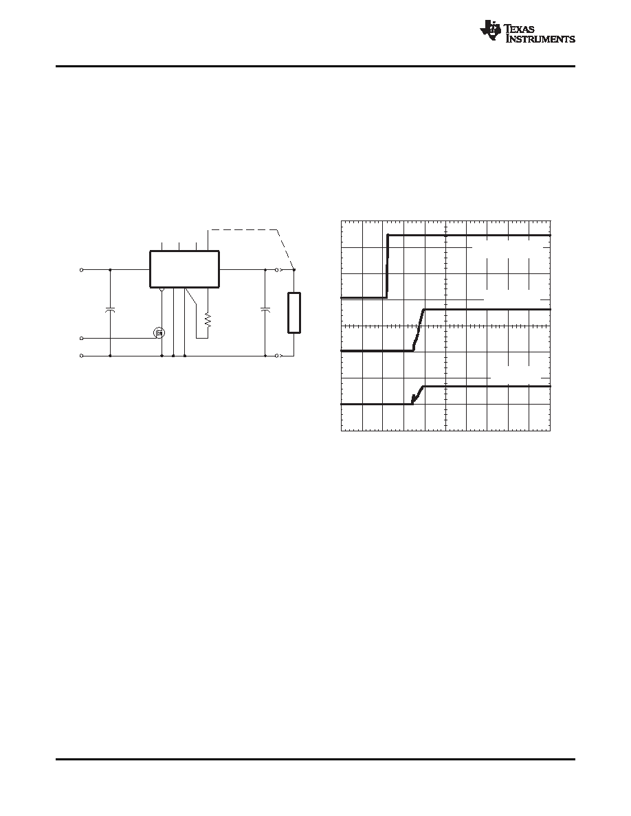
Figure 13 shows the typical application of the inhibit function. Note the discrete transistor (Q1). The Inhibit input
has its own internal pull-up to a potential of 5 V to 13.2 V (see footnotes to specification table). The input is not
compatible with TTL logic devices. An open-collector (or open-drain) discrete transistor is recommended for
control.
Figure 13. Inhibit Control Circuit
Figure 14. Power-Up from Inhibit Control
Turning Q1 on applies a low voltage to the Inhibit control pin and disables the output of the module. If Q1 is then
turned off, the module executes a soft-start power-up sequence. A regulated output voltage is produced within 25
ms Figure 14 shows the typical rise in both the output voltage and input current, following the turn-off of Q1. The
turn off of Q1 corresponds to the rise in the waveform, Q1 Vds. The waveforms were measured with a 5-A
constant current load.
Products with this feature incorporate an output voltage sense pin, VO Sense. A remote sense improves the load
regulation performance of the module by allowing it to compensate for any IR voltage drop between its output
and the load. An IR drop is caused by the high output current flowing through the small amount of pin and trace
resistance.
To use this feature simply connect the VO Sense pin to the VO node, close to the load circuit (see standard
application circuit). If a sense pin is left open-circuit, an internal low-value resistor (15-
or less) connected
between the pin and and the output node, ensures the output remains in regulation.
With the sense pin connected, the difference between the voltage measured directly between the VO and GND
pins, and that measured from VO Sense to GND, is the amount of IR drop being compensated by the regulator.
This should be limited to a maximum of 0.3 V.
Note: The remote sense feature is not designed to compensate for the forward drop of nonlinear or
frequency dependent components that may be placed in series with the converter output. Examples include
OR-ing diodes, filter inductors, ferrite beads, and fuses. When these components are enclosed by the remote
sense connection, they are effectively placed inside the regulation control loop, which can adversely affect
the stability of the regulator.
14
Copyright 2003–2008, Texas Instruments Incorporated
Product Folder Link(s): PTH12030W/L
相關(guān)PDF資料 |
PDF描述 |
|---|---|
| PTH12030WAZ | 1-OUTPUT DC-DC REG PWR SUPPLY MODULE |
| PTH12030LAH | 1-OUTPUT DC-DC REG PWR SUPPLY MODULE |
| PTH12030WAS | 1-OUTPUT DC-DC REG PWR SUPPLY MODULE |
| PTH12030LAST | 1-OUTPUT DC-DC REG PWR SUPPLY MODULE |
| PTH12030LAZT | 1-OUTPUT DC-DC REG PWR SUPPLY MODULE |
相關(guān)代理商/技術(shù)參數(shù) |
參數(shù)描述 |
|---|---|
| PTH12040 | 制造商:EMERSON-NETWORKPOWER 制造商全稱(chēng):Emerson Network Power 功能描述:DC-DC CONVERTERS |
| PTH12040W | 制造商:TI 制造商全稱(chēng):Texas Instruments 功能描述:50-A, 8-V to 14-V INPUT, NON-ISOLATED WIDE-OUTPUT ADJUST POWER MODULE |
| PTH12040WAD | 功能描述:DC/DC轉(zhuǎn)換器 50-A 8-14V-Inp Wide Out Adj Pwr Module RoHS:否 制造商:Murata 產(chǎn)品: 輸出功率: 輸入電壓范圍:3.6 V to 5.5 V 輸入電壓(標(biāo)稱(chēng)): 輸出端數(shù)量:1 輸出電壓(通道 1):3.3 V 輸出電流(通道 1):600 mA 輸出電壓(通道 2): 輸出電流(通道 2): 安裝風(fēng)格:SMD/SMT 封裝 / 箱體尺寸: |
| PTH12040WADT | 制造商:ARTESYN 制造商全稱(chēng):Artesyn Technologies 功能描述:DC-DC CONVERTERS POLA Non-isolated |
| PTH12040WAH | 功能描述:DC/DC轉(zhuǎn)換器 50-A 8-14V-Inp Wide Out Adj Pwr Module RoHS:否 制造商:Murata 產(chǎn)品: 輸出功率: 輸入電壓范圍:3.6 V to 5.5 V 輸入電壓(標(biāo)稱(chēng)): 輸出端數(shù)量:1 輸出電壓(通道 1):3.3 V 輸出電流(通道 1):600 mA 輸出電壓(通道 2): 輸出電流(通道 2): 安裝風(fēng)格:SMD/SMT 封裝 / 箱體尺寸: |
發(fā)布緊急采購(gòu),3分鐘左右您將得到回復(fù)。