- 您現(xiàn)在的位置:買賣IC網(wǎng) > PDF目錄378087 > PTF080601 (INFINEON TECHNOLOGIES AG) LDMOS RF Power Field Effect Transistor 60 W, 860-960 MHz PDF資料下載
參數(shù)資料
| 型號(hào): | PTF080601 |
| 廠商: | INFINEON TECHNOLOGIES AG |
| 英文描述: | LDMOS RF Power Field Effect Transistor 60 W, 860-960 MHz |
| 中文描述: | LDMOS射頻功率場(chǎng)效應(yīng)晶體管60瓦,860-960兆赫 |
| 文件頁數(shù): | 1/6頁 |
| 文件大小: | 293K |
| 代理商: | PTF080601 |
Developmental Data Sheet
1
2003-12-05
PTF080601A
Package 20248
PTF080601E
Package 30248
PTF080601F
Package 31248
-90
-80
-70
-60
-50
-40
-30
-20
32
34
36
38
40
42
44
46
Output Power (dBm)
M
5
10
15
20
25
30
35
40
45
50
E
V
DD
= 28 V, I
DQ
= 550 mA, f = 959.8 MHz
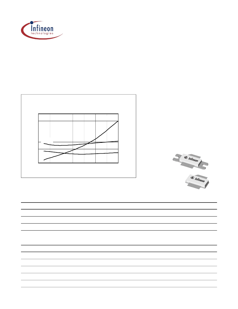
Typical EDGE Modulation Spectrum Performance
Mod Spectrum vs. Output Power
Efficiency
400KHz
600KHz
Developmental PTF080601
LDMOS RF Power Field Effect Transistor
60 W, 860–960 MHz
Features
Broadband internal matching
Typical EDGE performance
- Average output power = 30 W
- Gain = 18 dB
- Efficiency = 40%
Typical CW performance
- Output power at P–1dB = 90 W
- Gain = 17 dB
- Efficiency = 60%
Integrated ESD protection: Human Body
Model, Class 1 (minimum)
Excellent thermal stability
Low HCI drift
Capable of handling 10:1 VSWR @ 28 V,
60 W (CW) output power
RF Characteristics
at T
CASE
= 25°C unless otherwise indicated
Two-Tone Measurements
(tested in Infineon test fixture)
V
DD
= 28 V, I
DQ
= 550 mA, P
OUT
= 60 W PEP, f
C
= 960 MHz, tone spacing = 1000 kHz
Characteristic
Symbol
Min
Typ
Max
Units
Gain
G
ps
—
18
—
dB
Drain Efficiency
η
D
—
42
—
%
Intermodulation Distortion
IMD
—
–32
—
dBc
EDGE Measurements
(not subject to production test—verified by design/characterization in Infineon test fixture)
V
DD
= 28 V, I
DQ
= 550 mA, P
OUT
= 30 W, f = 959.8 MHz
Characteristic
Symbol
Min
Typ
Max
Units
Error Vector Magnitude
EVM (RMS)
—
2.0
—
%
Modulation Spectrum @ 400 KHz
ACPR
—
–61
—
dBc
Modulation Spectrum @ 600 KHz
ACPR
—
–74
—
dBc
Gain
G
ps
—
18
—
dB
Drain Efficiency
η
D
—
40
—
%
Description
The PTF080601 is a 60–W, internally matched
GOLDMOS
FET intended
for EDGE and CDMA applications in the 860 to 960 MHz band. Full gold
metallization ensures excellent device lifetime and reliability.
發(fā)布緊急采購,3分鐘左右您將得到回復(fù)。