- 您現(xiàn)在的位置:買賣IC網(wǎng) > PDF目錄368349 > PT7V2727 (Electronic Theatre Controls, Inc.) 3.3v/5.0v operating voltage PDF資料下載
參數(shù)資料
| 型號(hào): | PT7V2727 |
| 廠商: | Electronic Theatre Controls, Inc. |
| 英文描述: | 3.3v/5.0v operating voltage |
| 中文描述: | 3.3v/5.0v工作電壓 |
| 文件頁數(shù): | 1/5頁 |
| 文件大小: | 292K |
| 代理商: | PT7V2727 |
|||||||||||||||||||||||||||||||||||||||||||||||||||||||||||||||||||||||||||||||||||||||||||||||||||||||||||||||||||||||||||||||||||||||||||||||||||||||||||||||||||||||||||||||||||||||||||||||||||||||||||||||||||||||||||||||||||||||||||||||||||||||||||||||||||||||||||||||||||||||||||||||||||||||||||||||||||||||||||||||||||||||
Product Features
3.3v/5.0v
operating voltage
Uses an inexpensive external crystal
On-chip VCXO with pull range of 240ppm
VCXO tuning voltage from 0 to 3.3V
10mA output driver at CMOS levels
Available in SOIC package
Ordering Information
Ordering
code
type
Range
PT7V2727W
8-Pin SOIC
Industrial
PT7V3727W
8-Pin SOIC
Industrial
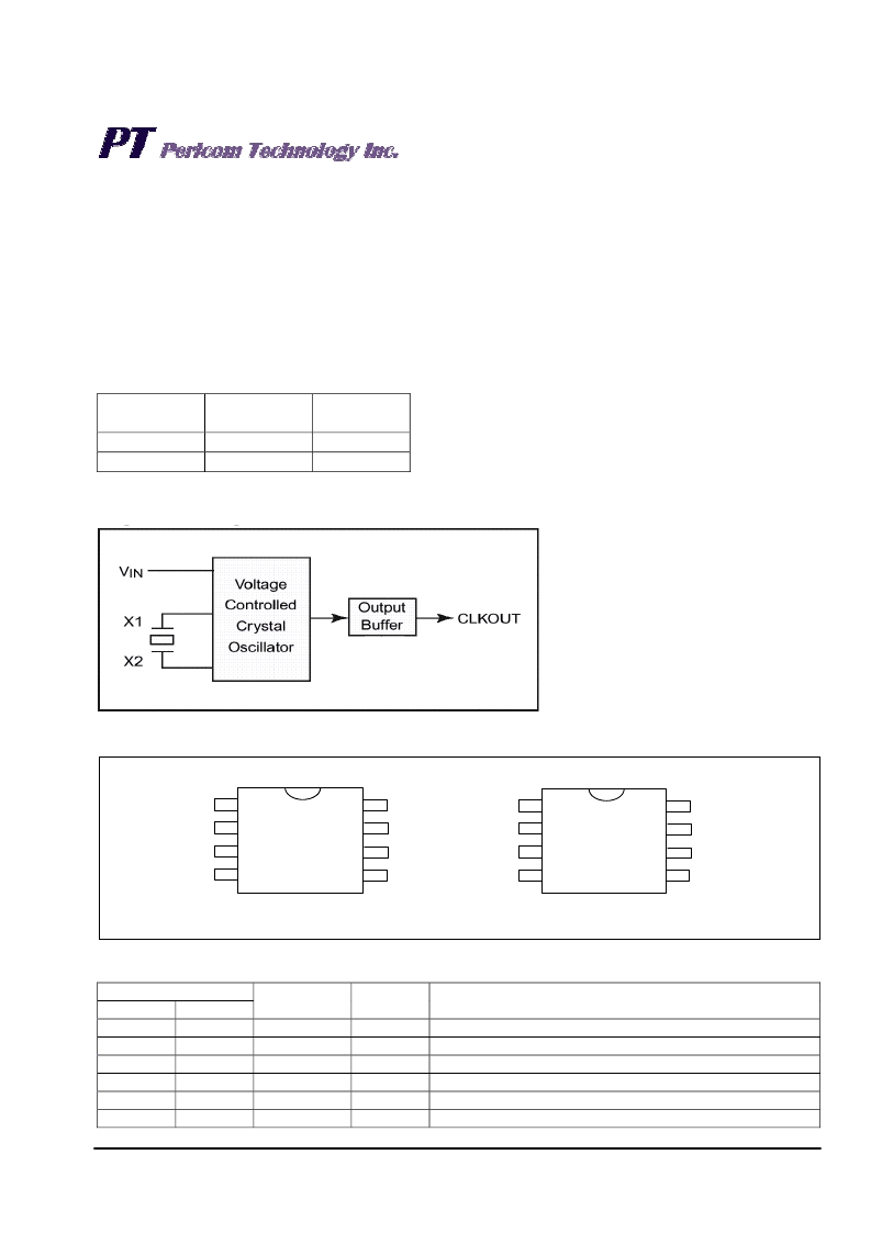
Logic Block Diagram
PT0173(05/04)
Ver: 0
1
Preliminary Data Sheet
PT7V2727/3727 VCXO
Package
Operating
Pin Configuration
Pin Description
Pin Number
2727
1, 8
2, 7
3
4
5
6
3727
1, 8
6
3
4, 7
5
2
Pin Name
Type
Description
X1, X2
NC
V
IN
GND
CLKOUT
V
CC
I
I
Crystal Connection, Connect to a pullable 27MHz crystal
No Connect, Can be float or connected to V
CC
or GND
Voltage Input to VCXO
Ground
Clock Output
Power Supply +
3.3v/
5.0
v
PWR
O
PWR
General Description
The PT7V2727/3727 are low-cost, high-performance 3.3V
/5.0v
VCXO, designed to replace expensive VCXO modules.
The on-chip voltage causes clocks to vary by ±120ppm.
They use an inexpensive external pullable crystal at
27MHz to produce the same output frequency.
Applications
Set-Top Box
xDSL
z
z
1
2
3
4
5
6
7
8
X1
VIN
GND
NC
X2
NC
Vcc
PT7V2727
SOIC 8 package
CLKOUT
1
2
3
4
5
6
7
8
X1
VIN
GND
Vcc
X2
GND
NC
CLKOUT
PT7V3727
SOIC 8 package
相關(guān)PDF資料 |
PDF描述 |
|---|---|
| PT7V2727W | 3.3v/5.0v operating voltage |
| PT7V3727W | 3.3v/5.0v operating voltage |
| PT7V4027W | 3.3V operating voltage |
| PT7V4027 | 20V Dual N- and P- Channel HEXFET Power MOSFET in a SO-8 package |
| PT7V4050 | PLL with quartz stabilized VCXO? |
相關(guān)代理商/技術(shù)參數(shù) |
參數(shù)描述 |
|---|---|
| PT7V2727W | 制造商:未知廠家 制造商全稱:未知廠家 功能描述:3.3v/5.0v operating voltage |
| PT7V3727W | 制造商:未知廠家 制造商全稱:未知廠家 功能描述:3.3v/5.0v operating voltage |
| PT7V4027 | 制造商:未知廠家 制造商全稱:未知廠家 功能描述:3.3V operating voltage |
| PT7V4027W | 制造商:未知廠家 制造商全稱:未知廠家 功能描述:3.3V operating voltage |
| PT7V4027WE | 制造商:Pericom Semiconductor Corporation 功能描述: |
發(fā)布緊急采購,3分鐘左右您將得到回復(fù)。