- 您現(xiàn)在的位置:買(mǎi)賣(mài)IC網(wǎng) > PDF目錄66056 > PT7712C (TEXAS INSTRUMENTS INC) 20 A SWITCHING REGULATOR, 400 kHz SWITCHING FREQ-MAX, MSMA27 PDF資料下載
參數(shù)資料
| 型號(hào): | PT7712C |
| 廠商: | TEXAS INSTRUMENTS INC |
| 元件分類(lèi): | 穩(wěn)壓器 |
| 英文描述: | 20 A SWITCHING REGULATOR, 400 kHz SWITCHING FREQ-MAX, MSMA27 |
| 封裝: | METAL, SMD-27 |
| 文件頁(yè)數(shù): | 2/9頁(yè) |
| 文件大?。?/td> | 183K |
| 代理商: | PT7712C |
For technical support and more information, see inside back cover or visit www.ti.com
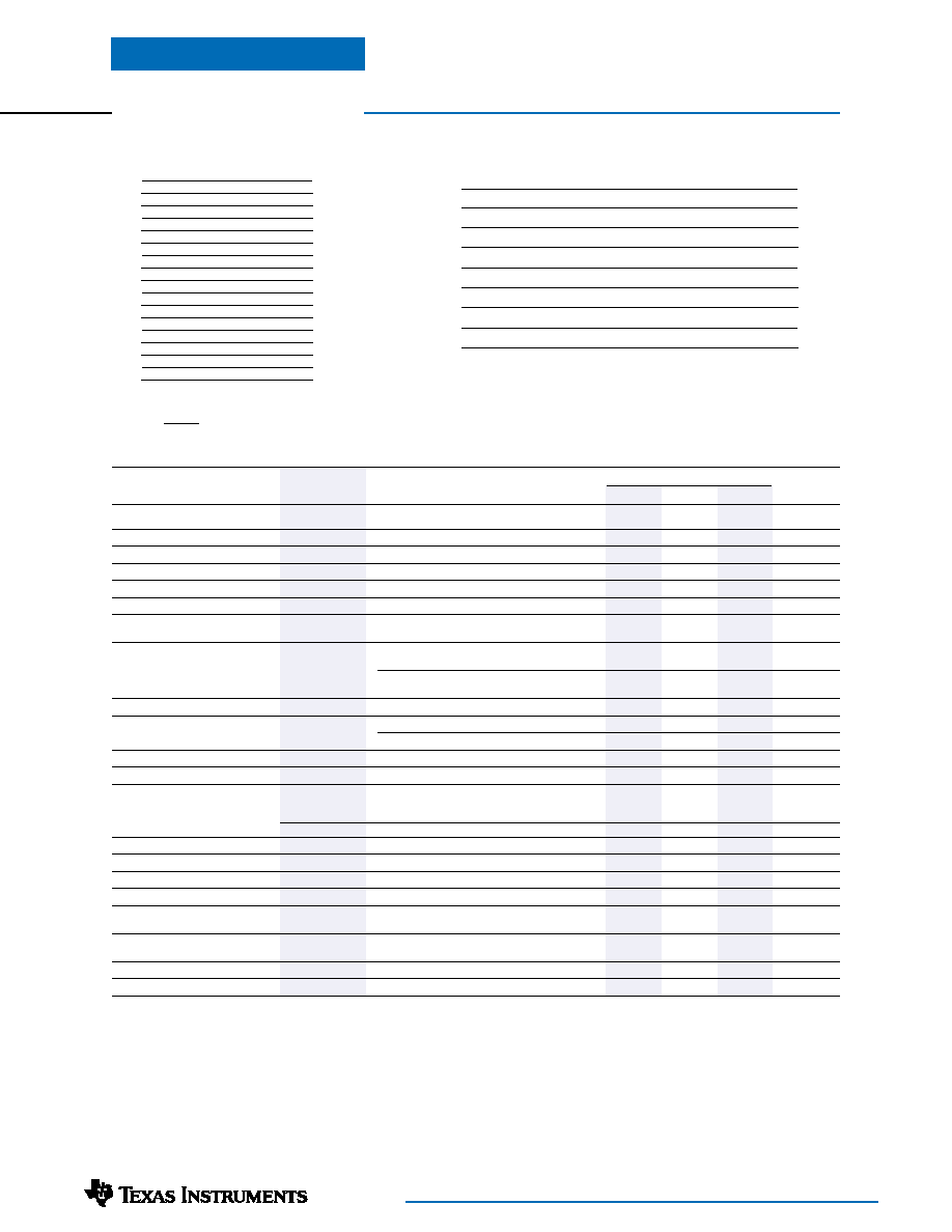
PT7710 Product Family Comparison
Input
Adjust
Output
Product
Voltage
Description
Method
Range
PT7711
5V
VID
5-Bit
1.3V– 3.5V
PT7712
3.3V
VID
4-Bit
1.3V– 2.05V
PT7713
3.3V
VID
4-Bit
1.8V– 2.55V
PT7714
3.3V
VID
5-Bit
0.8V–1.575V
PT7715
5V
VID
5-Bit
1.075V–1.85V
PT7716
3.3V
VID
5-Bit
1.075V–1.85V
PT7744
3.3V
Booster
—
PT7745
5V
Booster
—
PT7712—3.3V
20-A Programmable
Integrated Switching Regulator
Programming Information
VID3 VID2 VID1 VID0
Vout
111
1
1.30V
111
0
1.35V
110
1
1.40V
110
0
1.45V
101
1
1.5V
101
0
1.55V
100
1
1.60V
1
0
1.65V
0
1
1.70V
0
1
0
1.75V
0
1
0
1
1.80V
0
1
0
1.85V
0
1
1.90V
0
1
0
1.95V
0
1
2.00V
0
2.05V
Logic 0 = Pin 12 potential (remote sense gnd)
Logic 1 = Open circuit (no pull-up resistors)
VID3 must not be changed while the unit is operating.
Specifications (Unless otherwise stated, Ta =25°C, Vin =3.3V, Cin =1,500F, Cout =330F, Vo =1.8V, and Io =Iomax)
PT7712
Characteristics
Symbols
Conditions
Min
Typ
Max
Units
Output Current
Io
Ta = +25°C, Natural convection
0.1 (1)
—20
A
Ta = +60°C, 200 LFM, pkg N
0.1 (1)
—19
Input Voltage Range
Vin
Over Io range
3.1
—
3.6
V
Set-Point Voltage Tolerance
Vo tol
All output voltages
—
±10
±25 (2)
mV
Temperature Variation
Regtemp
–40°C
≤Ta ≤+85°C, Io =Iomin
—
±0.75
—
%Vo
Line Regulation
Regline
Over Vin range
—
±5
—
mV
Load Regulation
Regload
Over Io range
—
±5
—
mV
Total Output Voltage Variation
Vo tol
Includes set-point, line, load,
—
±1±3%Vo
–40°C
≤Ta ≤+85°C
Efficiency
η
Io =10A
Vo =1.8V
—
87
—
%
Vo =1.5V
—
85
—
Io =20A
Vo =1.8V
—
83
—
%
Vo =1.5V
—
81
—
Vo Ripple (pk-pk)
Vr
20MHz bandwidth
—
50
—
mVpp
Transient Response
ttr
1A/s load step, 50% and 100% Iomax
—
50
—
Sec
Vos
Vo over/undershoot
—
±100
—
mV
Over-Current Threshold
ITRIP
Reset followed by auto-recovery
—
32
—
A
Switching Frequency
o
Over Vin range
300
350
400
kHz
STBY* Input Requirements
Referenced to GND
Input High Voltage
VIH
2.0
—
Open (3)
V
Input Low Voltage
VIL
-0.2
—
0.8
Input Low Current
IIL
Pin 5 to GND
—
0.3
—
mA
Standby Input Current
Iin standby
Pin 5 to GND
—
30
—
mA
External Capacitance
Cout
330 (4)
—
15,000
F
Operating Temperature Range
Ta
Over Vin Range
–40
—
+85 (5)
°C
Storage Temperature
Ts
—
-40
—
+125
°C
Mechanical Shock
—
Per Mil-STD-883D, Method 2002.3
—
500
—
G’s
1 msec, Half Sine, mounted to a fixture
Mechanical Vibration
—
Mil-STD-883D, Method 2007.2
Suffixes N, A
—
20 (6)
—
G’s
20-2000 Hz
Suffix C
—
15 (6)
—
Weight
—
Vertical/Horizontal
—
36
—
grams
Flammability
—
Materials meet UL 94V-0
Notes: (1) ISR-will operate down to no load with reduced specifications.
(2) If the remote sense ground is not used, pin 12 must be connected to pin 13 for optimum output voltage accuracy.
(3) The STBY* control (pin 5) has an internal pull-up. If it is left open-circuit, the module will operate when input power is applied. A low-leakage (<1A)
MOSFET must be used to control this pin. The open-circuit voltage may be as high as Vin.
(4) For operation below 0°C, Cin and Cout must have stable characteristics. Use either low ESR tantalum or Oscon capacitors.
(5) See safe Operating Area curves or consult factory for the appropriate derating.
(6) The case pins on the through-hole package types (suffixes N & A) must be soldered. For more information see the applicable package outline drawing.
External Capacitors: The regulator requires a minimum output capacitance of 330F for proper operation. An input capacitance of 1500F is also required. This
must be rated for a minimum of 1.4Arms of ripple current. For transient or dynamic load applications, additional capacitance may be required. For further informa-
tion refer to the application note regarding capacitor selection for this product.
Input Filter: An input filter inductor is optional for most applications. The inductor must be sized to handle 20ADC with a typical value of 1H.
相關(guān)PDF資料 |
PDF描述 |
|---|---|
| PT7713C | 20 A SWITCHING REGULATOR, 400 kHz SWITCHING FREQ-MAX, MSMA27 |
| PT7713N | 20 A SWITCHING REGULATOR, 400 kHz SWITCHING FREQ-MAX, MSMA27 |
| PT7713A | 20 A SWITCHING REGULATOR, 400 kHz SWITCHING FREQ-MAX, MSMA27 |
| PT7740A | 1-OUTPUT DC-DC BOOSTER MODULE |
| PT7740C | 1-OUTPUT DC-DC BOOSTER MODULE |
相關(guān)代理商/技術(shù)參數(shù) |
參數(shù)描述 |
|---|---|
| PT7712N | 功能描述:開(kāi)關(guān)變換器、穩(wěn)壓器與控制器 20A 3.3Vin Next Gen Programmable ISR RoHS:否 制造商:Texas Instruments 輸出電壓:1.2 V to 10 V 輸出電流:300 mA 輸出功率: 輸入電壓:3 V to 17 V 開(kāi)關(guān)頻率:1 MHz 工作溫度范圍: 安裝風(fēng)格:SMD/SMT 封裝 / 箱體:WSON-8 封裝:Reel |
| PT7712VD | 制造商:TI 制造商全稱(chēng):Texas Instruments 功能描述:20-A Programmable Integrated Switching Regulator |
| PT7713 | 制造商:未知廠家 制造商全稱(chēng):未知廠家 功能描述:20-A 1.8V to 2.55V 3.3V-Input Programmable ISR |
| PT7713A | 功能描述:DC/DC轉(zhuǎn)換器 20A 1.8V-2.55V 3.3V Programmable ISR RoHS:否 制造商:Murata 產(chǎn)品: 輸出功率: 輸入電壓范圍:3.6 V to 5.5 V 輸入電壓(標(biāo)稱(chēng)): 輸出端數(shù)量:1 輸出電壓(通道 1):3.3 V 輸出電流(通道 1):600 mA 輸出電壓(通道 2): 輸出電流(通道 2): 安裝風(fēng)格:SMD/SMT 封裝 / 箱體尺寸: |
| PT7713C | 功能描述:REG 1.8-2.55V 20A 3.3VIN SMD RoHS:否 類(lèi)別:電源 - 板載 >> DC DC Converters 系列:PT7710 設(shè)計(jì)資源:Maxi/Mini/Micro Design Guide, Appl Manual 標(biāo)準(zhǔn)包裝:1 系列:Maxi 類(lèi)型:隔離 輸出數(shù):1 電壓 - 輸入(最?。?43V 電壓 - 輸入(最大):110V Voltage - Output 1:15V Voltage - Output 2:- Voltage - Output 3:- 電流 - 輸出(最大):* 電源(瓦) - 制造商系列:400W 電壓 - 隔離:* 特點(diǎn):* 安裝類(lèi)型:通孔 封裝/外殼:模塊 尺寸/尺寸:4.60" L x 2.20" W x 0.54" H(116.8mm x 55.9mm x 13.7mm) 包裝:散裝 工作溫度:-55°C ~ 100°C 效率:* 電源(瓦特)- 最大:* |
發(fā)布緊急采購(gòu),3分鐘左右您將得到回復(fù)。