- 您現(xiàn)在的位置:買賣IC網(wǎng) > PDF目錄368341 > PT5062R Analog IC PDF資料下載
參數(shù)資料
| 型號(hào): | PT5062R |
| 英文描述: | Analog IC |
| 中文描述: | 模擬IC |
| 文件頁(yè)數(shù): | 3/4頁(yè) |
| 文件大?。?/td> | 114K |
| 代理商: | PT5062R |
Application Notes
For technical support and more information, see inside back cover or visit www.ti.com
PT5060 Series
Adjusting the Output Voltage of the PT5060
Dual-Output Boost Converter Series
The dual output voltage of the PT5060 series modules
can be adjusted higher or lower than the factory pre-set
voltage with the addition of a single external resistor.
Table 1 gives the applicable adjustment range for each
model in the series as V
a
(min) and V
a
(max).
Adjust Up:
An increase in the output voltage is obtained
by adding a resistor R
2
, between pin 11 (V
o
adj) and pins
2, 6, or 7 (GND).
Adjust Down:
Add a resistor
(R
1
)
, between pin 11 (V
o
adj)
and pins 8, 9 or 10 (Vo
1
).
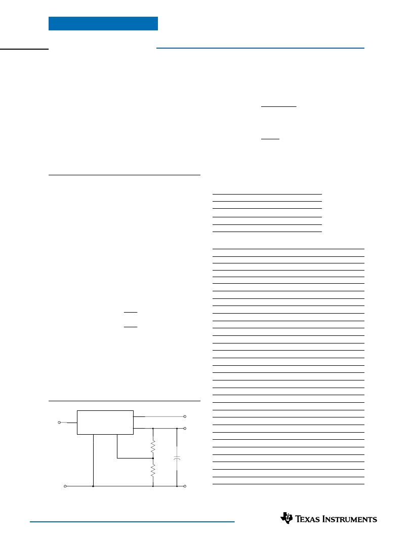
Refer to Figure 1 and Table 2 for both the placement and value
of the required resistor, either
(R
1
)
or R
2
as appropriate.
Notes:
1. Both the positive and negative voltage outputs from the
ISR are adjusted simultaneously.
2. Use only a single 1% resistor in either the
(R
1
)
or R
2
location. Place the resistor as close to the ISR as possible.
3. Never connect capacitors from V
o
adj to either GND or
V
o
. Any capacitance added to the V
o
adjust pin will affect
the stability of the ISR.
4. An increase in the output voltage must be accompanied by
a corresponding reduction in the specified maximum
current at each output. For Vo
1
and –Vo
2
, the revised
maximum output current must be reduced to the
equivalent of 6 watts and 3 watts respectively. i.e.
Io
1
(max)
=
6
V
a
3
V
a
Adc
and
Io
2
(max)
=
Adc,
where V
a
is the adjusted output voltage.
5. Adjustments to the output voltage will also limit the
maximum input voltage that can be applied to the ISR.
The maximum input voltage that may be applied is limited
to (V
o
– 1)Vdc or 14Vdc, whichever is less.
Table 1
PT5060 ADJUSTMENT AND FORMULA PARAMETERS
Series Pt #
PT5061
PT5062
Vo (nom)
Va (min)
Va (max)
±12.0V
± 7.5V
±14.0V
±15.0V
± 7.5V
±20.0V
The values of
(R
1
)
[adjust down], and R
2
[adjust up], can
also be calculated using the following formulas.
3.65 (V
a
– 2.5
)
(V
o
– V
a
)
(R
1
)
=
- 0.1
k
9.125
V
a
- V
o
- 0.1
k
R
2
=
Where:
V
o
V
a
= Original output voltage
= Adjusted output voltage
Figure 1
Table 2
PT5060 ADJUSTMENT RESISTOR VALUES
Series Pt #
Current
V
o
(nom)
V
a
(req
’
d)
7.0
7.5
8.0
8.5
9.0
9.5
10.0
10.5
11.0
11.5
12.0
12.5
13.0
13.5
14.0
14.5
15.0
15.5
16.0
16.5
17.0
17.5
18.0
18.5
19.0
19.5
20.0
R
1
=
(Blue)
PT5061
0.5/0.25Adc
±12.0Vdc
PT5062
0.4/0.2Adc
±15.0Vdc
(4.0)k
(4.9)k
(6.2)k
(7.8)k
(10.1)k
(13.6)k
(19.4)k
(30.9)k
(65.6)k
(2.3)k
(2.8)k
(3.3)k
(3.9)k
(4.6)k
(5.4)k
(6.4)k
(7.7)k
(9.3)k
(11.5)k
(14.5)k
(19.1)k
(26.7)k
(41.9)k
(87.5)k
18.2k
9.0k
6.0k
4.5k
18.2k
9.0k
6.0k
4.5k
3.6k
2.9k
2.5k
2.2k
1.9k
1.7k
R
2
= Black
C
out
100
μ
F
+
R
Adjust Up
(R
)
Adj Down
–
Vo
2
COM
V
in
COM
+Vo
1
PT5060
1
2,6,7
3,4,5
Vin
–
Vo
2
GND
11
Vo(adj)
8,9,10
+Vo
1
相關(guān)PDF資料 |
PDF描述 |
|---|---|
| PT5061A | 30V Single N-Channel HEXFET Power MOSFET in a D2-Pak package; A IRL3803S with Standard Packaging |
| PT5061B | Analog IC |
| PT5061C | Analog IC |
| PT5061G | Analog IC |
| PT5061N | 100V Single N-Channel HEXFET Power MOSFET in a TO-220AB package; A IRF540NPBF with Standard Packaging |
相關(guān)代理商/技術(shù)參數(shù) |
參數(shù)描述 |
|---|---|
| PT5065 | 功能描述:變壓器音頻和信號(hào) ISDN U XFMR;SGS TH & NAT’L;RM CORE RoHS:否 制造商:Skyworks Solutions, Inc. 頻率范圍:810 MHz to 960 MHz 初級(jí)線圈阻抗: 次級(jí)線圈阻抗: 絕緣電壓:23 dB 工作溫度范圍:- 40 C to + 85 C 端接類型:SMD/SMT 尺寸:6 mm L x 4.9 mm W x 1.6 mm H 產(chǎn)品:Splitters and Combiners |
| PT506-5 | 制造商:未知廠家 制造商全稱:未知廠家 功能描述:TRIAC|500V V(DRM)|6A I(T)RMS|TO-5VAR |
| PT506-66 | 制造商:未知廠家 制造商全稱:未知廠家 功能描述:TRIAC|500V V(DRM)|6A I(T)RMS|TO-66 |
| PT5069 | 功能描述:變壓器音頻和信號(hào) ISDN DUAL XFMR RoHS:否 制造商:Skyworks Solutions, Inc. 頻率范圍:810 MHz to 960 MHz 初級(jí)線圈阻抗: 次級(jí)線圈阻抗: 絕緣電壓:23 dB 工作溫度范圍:- 40 C to + 85 C 端接類型:SMD/SMT 尺寸:6 mm L x 4.9 mm W x 1.6 mm H 產(chǎn)品:Splitters and Combiners |
| PT506S | 制造商:未知廠家 制造商全稱:未知廠家 功能描述:TRIAC|500V V(DRM)|6A I(T)RMS|TO-208VAR1/2 |
發(fā)布緊急采購(gòu),3分鐘左右您將得到回復(fù)。