- 您現(xiàn)在的位置:買賣IC網(wǎng) > PDF目錄98061 > PT4661N (TEXAS INSTRUMENTS INC) 2-OUTPUT 25 W DC-DC REG PWR SUPPLY MODULE PDF資料下載
參數(shù)資料
| 型號: | PT4661N |
| 廠商: | TEXAS INSTRUMENTS INC |
| 元件分類: | 電源模塊 |
| 英文描述: | 2-OUTPUT 25 W DC-DC REG PWR SUPPLY MODULE |
| 文件頁數(shù): | 10/16頁 |
| 文件大小: | 321K |
| 代理商: | PT4661N |
For technical support and further information, visit http://power.ti.com
PT4660 Series
30-A Dual Output Isolated
DC/DC Converter
SLTS140C – MAY 2001 – REVISED OCTOBER 2003
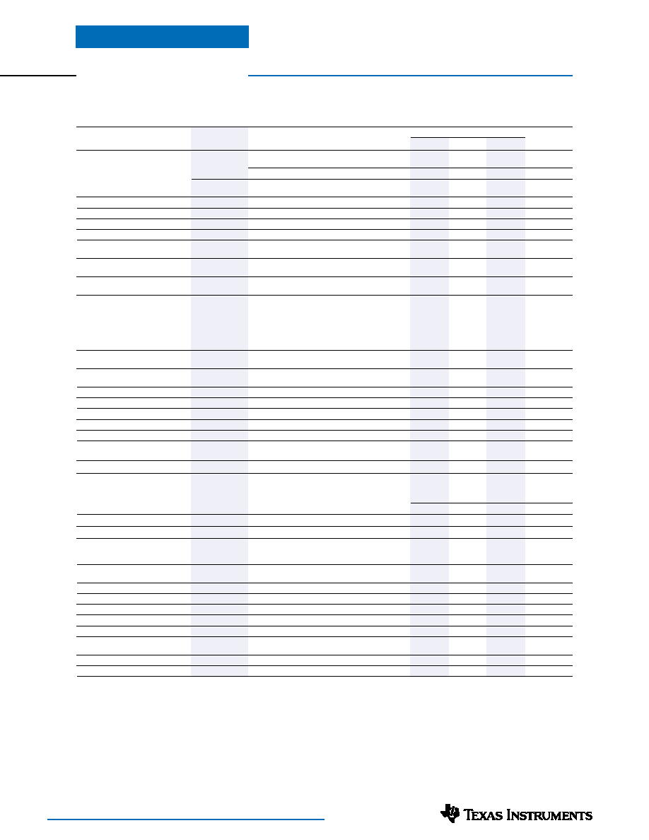
Specifications (Unless otherwise stated, Ta =25 °C, Vin =48 V, & Io1=Io2=10 A)
PT4660 SERIES
Characteristics
Symbols
Conditions
Min
Typ
Max
Units
Output Current
Io1, Io2
Vo1
Vo1 ≤3.3 V
0
—
15
A
Vo1 =5.0 V
0
—
10
Vo2
All voltages
0
—
15
A
Io1+Io2
Total (both outputs)
Vo1 ≤3.3 V
0
—
30
A
Vo1 =5.0 V
0
—
25
Input Voltage Range
Vin
36
48
75
V
Set Point Voltage Tolerance
Votol
—
±1±2%Vo
Temperature Variation
Regtemp
–40 to +100 °C Case, Io1 =Io2 =0 A
—
±0.5
—
%Vo
Line Regulation
Regline
Over Vin range with Io1=Io2=5 A
—
±5
±10
mV
Load Regulation
Regload
1 A
≤Io1 ≤Io1max, Io2 =1 A
Vo1
—
±2
±10
mV
1 A
≤Io2 ≤Io1max, Io1 =1 A
Vo2
—
±2
±10
Cross Regulation
Regcross
1 A
≤Io2 ≤Io1max, Io1 =1 A
Vo1
—
±2
±10
mV
1 A
≤Io1 ≤Io1max, Io2 =1 A
Vo2
—±2
±5
Total Output Variation
Votol
Includes set-point, line load,
Vo1
—±2
±3
%Vo
–40 °C to +100 °C case
Vo2
—±2
±3
Efficiency
η
PT4661
—
88
—
PT4662
—
87
—
PT4663
—
86
—
PT4665
—
86
—
%
PT4666
—
85
—
PT4667
—
88
—
PT4668
—
86
—
Vo Ripple (pk-pk)
Vr
Io1=Io2=5 A, 20 MHz bandwidth
Vo =5 V
—
75
mVpp
Vo <5 V
—
50
Transient Response
ttr
1 A/s load step from 50 % to 100 % Iomax
—
25
100
Sec
(either output)
—
6.0
—
%Vo
Current Limit
ILIM
Each output with other unloaded
15.5
18
—
A
Output Rise Time
ton
At turn-on to within 90 % of Vo
—
5
10
mSec
Output Over-Voltage Protection
OVP
Either output; shutdown and latch off
—
125 (1)
—%Vo
Output Voltage Adjustment
Voadj
Vo1, Vo2
—
±10
—
%Vo
Switching Frequency
fs
270
—
330
kHz
Under-Voltage-Lockout
UVLO
Rising
—
34
36
V
Falling
30
32
—
Internal Input Capacitance
Cin
—2
—F
Enable Control Inputs
Referenced to –Vin
Input High Voltage
VIH
3.5
—
V
Input Low Voltage
VIL
0
—
0.8 (2)
Input Low Current
IIL
—
0.5
—
mA
Standby Current
Iin standby
Pins 2, 3, & 4 connected
—
3
5
mA
External Output Capacitance
Cout
Per each output
0
—
5,000
F
Primary/Secondary Isolation
V iso
1500
—
V
C iso
—
1500
—
pF
R iso
10
——M
Temperature Sense
Vtemp
Output voltage at temperatures:-
–40 °C
—
0.1 (3)
—
V
100 °C
—
1.5 (3)
—
Operating Temperature Range
Ta
Over Vin range
–40
—
85 (4)
°C
Over-Temperature ProtectionOTP
Case temperature (auto restart)
100
—
°C
Solder Reflow Temperature
Treflow
Surface temperature of module pins or case
—
215 (5)
°C
Storage Temperature
Ts
—
–40
—
125
°C
Mechanical Shock
—
Per Mil-STD-883D, Method 2002.3
—
500
—
G’s
Mechanical Vibration
—
Per Mil-STD-883D, Method 2007.2, Suffix N
—
10 (6)
—
G’s
20–2,000 Hz
Suffixes A, C
—
20 (6)
—
Weight
—
90
—
grams
Flammability
—
Materials meet UL 94V-0
Notes: (1) This is a fixed parameter. Adjusting Vo1 or Vo2 higher will increase the module’s sensitivity to over-voltage detection. For more information, see the
application note on output voltage adjustment.
(2) The EN1 and EN2 control inputs (pins 3 & 4) have internal pull-ups and may be controlled with an open-collector (or open-drain) transistor. Both
inputs are diode protected and can be connected to +Vin. The maximum open-circuit voltage is 5.4 V.
(3) Voltage output at “TEMP” pin is defined by the equation:- VTEMP = 0.5 + 0.01T, where T is in °C. See pin descriptions for more information.
(4) See SOA curves or consult the factory for the appropriate derating.
(5) During solder reflow of SMD package version do not elevate the module case, pins, or internal component temperatures above a peak of 215 °C. For
further guidance refer to the application note, “Reflow Soldering Requirements for Plug-in Power Surface Mount Products,” (SLTA051).
(6) The case pins on the through-holed package types (suffixes N & A) must be soldered. For more information see the applicable package outline drawing.
相關(guān)PDF資料 |
PDF描述 |
|---|---|
| PT4663A | 2-OUTPUT 25 W DC-DC REG PWR SUPPLY MODULE |
| PT4661C | 2-OUTPUT 25 W DC-DC REG PWR SUPPLY MODULE |
| PT4662C | 2-OUTPUT 25 W DC-DC REG PWR SUPPLY MODULE |
| PT4663C | 2-OUTPUT 25 W DC-DC REG PWR SUPPLY MODULE |
| PT4662N | 2-OUTPUT 25 W DC-DC REG PWR SUPPLY MODULE |
相關(guān)代理商/技術(shù)參數(shù) |
參數(shù)描述 |
|---|---|
| PT4662 | 制造商:TI 制造商全稱:Texas Instruments 功能描述:30-A Dual Output Isolated DC/DC Converter |
| PT4662A | 功能描述:直流/直流開關(guān)轉(zhuǎn)換器 3.3/2.5V 30A/2-Out 48V Inp Iso DC/DC RoHS:否 制造商:STMicroelectronics 最大輸入電壓:4.5 V 開關(guān)頻率:1.5 MHz 輸出電壓:4.6 V 輸出電流:250 mA 輸出端數(shù)量:2 最大工作溫度:+ 85 C 安裝風(fēng)格:SMD/SMT |
| PT4662C | 功能描述:DC/DC轉(zhuǎn)換器 3.3/2.5V 30A/2-Out 48V Inp Iso DC/DC RoHS:否 制造商:Murata 產(chǎn)品: 輸出功率: 輸入電壓范圍:3.6 V to 5.5 V 輸入電壓(標(biāo)稱): 輸出端數(shù)量:1 輸出電壓(通道 1):3.3 V 輸出電流(通道 1):600 mA 輸出電壓(通道 2): 輸出電流(通道 2): 安裝風(fēng)格:SMD/SMT 封裝 / 箱體尺寸: |
| PT4662N | 功能描述:直流/直流開關(guān)轉(zhuǎn)換器 3.3/2.5V 30A/2-Out 48V Inp Iso DC/DC RoHS:否 制造商:STMicroelectronics 最大輸入電壓:4.5 V 開關(guān)頻率:1.5 MHz 輸出電壓:4.6 V 輸出電流:250 mA 輸出端數(shù)量:2 最大工作溫度:+ 85 C 安裝風(fēng)格:SMD/SMT |
| PT4663 | 制造商:TI 制造商全稱:Texas Instruments 功能描述:20-A 24-V Input Dual Output Isolated DC/DC Converter |
發(fā)布緊急采購,3分鐘左右您將得到回復(fù)。