- 您現(xiàn)在的位置:買賣IC網(wǎng) > PDF目錄370024 > PT4471 100W 24V Input 30A Programmable DC-DC Converter PDF資料下載
參數(shù)資料
| 型號: | PT4471 |
| 元件分類: | DC/DC變換器 |
| 英文描述: | 100W 24V Input 30A Programmable DC-DC Converter |
| 中文描述: | 100W的24V輸入30A條可編程DC - DC轉(zhuǎn)換器 |
| 文件頁數(shù): | 6/7頁 |
| 文件大小: | 157K |
| 代理商: | PT4471 |
For technical support and more information, see inside back cover or visit www.ti.com
Application Notes
Using the Inhibit Function on the PT4470 &
PT4480 Series of Isolated DC/DC Converters
The PT4470/44480 series of DC/DC converters incor-
porate an On/Off Inhibit function. This function may be
used in applications that demand battery conservation,
power-up/shutdown sequencing, and/or to coordinate
power-up for active in-rush current control.
The On/Off feature is provided by the
Inhibit
control,
pin 3. The
Inhibit
pin of the PT4470/4480 series of
converters is an active low enable. The pin must be
either connected, or actively pulled low, to –V
in
(pin 2)
to enable the converter output (see standard applica-
tion schematic). When pins 2 & 3 are connected, the
converter provides a regulated output whenever a valid
source voltage
3
is applied between +V
in
(pin 1), and –V
in
(pin 2). If pin 3 is disconnected, or allowed to become
high impedance, the regulator output will be disabled.
5
Table 2-1 provides details of the interface requirements
for the
Inhibit
pin. Figure 2-1 shows how a discrete
MOSFET (Q
1
)
4
, may be referenced to –V
in
and used to
control the input.
Table 2-1 Inhibit Control Requirements
Parameter
Enable (V
IH
)
Disable (V
IL
)
Min
–0.5V
2.5V
Max
0.8V
(Open Circuit)
Notes:
1.
The
Inhibit
control uses –V
in
(pin 2), on the primary side
of the converter, as its ground reference. All voltages
specified are with respect to –V
in
.
2. The internal circuitry is simple pull-up resistor. The
open-circuit voltage may be as high as 6.5Vdc.
3. These converters incorporate an “Under-Voltage
Lockout” (UVLO) function. This function automatically
disables the converter output until there is sufficient input
voltage to produce a regulated output. Table 2 gives the
applicable UVLO thresholds.
Table 2-2 UVLO Thresholds
1
Series
PT4470
PT4480
UVLO Threshold
17.0V Typical
34.5V Typical
V
in
Range
18 – 36V
36 – 75V
4.
The
Inhibit
input must be controlled with an open-
collector (or open-drain) discrete transistor or
MOSFET.
Do not
use a pull-up resistor.
5. When the converter output is disabled, the current
drawn from the input supply is typically reduced to
4mA (10mA maximum).
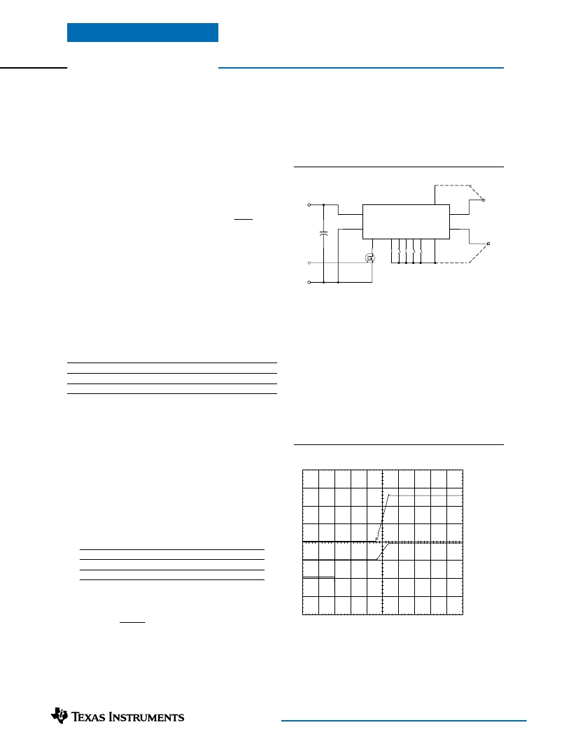
Figure 2-1
Turn-On Time:
With input power applied, the converter
typically produces a fully regulated output voltage within
25ms after applying a low-voltage signal to the
Inhibit
control pin. The actual turn-on time will vary with
the input voltage, output load, and the total amount of
capacitance connected to the output. Using the circuit of
Figure 2-1, Figure 2-2 shows the typical output voltage
and input current waveforms of a PT4472 after Q
1
is
turned on. The turn on of Q
1
correlates to the fall in
V
inh
. The output voltage was set to 2.5V. The waveform
was measured with a 48-Vdc input voltage, and 15-A load
current.
Figure 2-2
PT4470, PT4480 Series
6. Keep the on/off transition to less than 1ms. This
prevents erratic operation of the ISR, whereby the
output voltage may drift un-regulated between 0V
and the rated output during power-up.
Vout (1V/Div)
Iin (2A/Div)
Vinh (5V/Div)
HORIZ SCALE: 5ms/Div
PT4472
+V
sns
+V
out
-V
out
-V
sns
7
8-13
14-19
20
21
25
22
24
23
VID0 - VID4
+V
in
–
V
in
1
2
3
Inhibit
C
1
+
PROGRAMMING PINS
+2.5V
+V
IN
–
V
IN
0V
1 =Enable
Q
BSS138
相關(guān)PDF資料 |
PDF描述 |
|---|---|
| PT46X150 | 20V Single N-Channel HEXFET Power MOSFET in a TO-220AB package; Similar to IRF3711Z with Lead Free Packaging |
| PT46X150-KNE | 100V Single N-Channel HEXFET Power MOSFET in a TO-220AB package; A IRF540ZPBF with Standard Packaging |
| PT46X250MM | THERMOSONDE PT100 PTFE ISOLIERT 250MM |
| PT46X300-KNE | THERMOSENSOR MIT ANSCHLUSSKOPF 300MM |
| PT4701 | 150V Single N-Channel HEXFET Power MOSFET in a SO-8 package; A IRF7451 with Standard Packaging |
相關(guān)代理商/技術(shù)參數(shù) |
參數(shù)描述 |
|---|---|
| PT4471A | 功能描述:直流/直流開關(guān)轉(zhuǎn)換器 100W 24V In 30A Prog DC-DC Converter RoHS:否 制造商:STMicroelectronics 最大輸入電壓:4.5 V 開關(guān)頻率:1.5 MHz 輸出電壓:4.6 V 輸出電流:250 mA 輸出端數(shù)量:2 最大工作溫度:+ 85 C 安裝風(fēng)格:SMD/SMT |
| PT4471C | 功能描述:直流/直流開關(guān)轉(zhuǎn)換器 100W 24V In 30A Prog DC-DC Converter RoHS:否 制造商:STMicroelectronics 最大輸入電壓:4.5 V 開關(guān)頻率:1.5 MHz 輸出電壓:4.6 V 輸出電流:250 mA 輸出端數(shù)量:2 最大工作溫度:+ 85 C 安裝風(fēng)格:SMD/SMT |
| PT4471N | 功能描述:直流/直流開關(guān)轉(zhuǎn)換器 100W 24V In 30A Prog DC-DC Converter RoHS:否 制造商:STMicroelectronics 最大輸入電壓:4.5 V 開關(guān)頻率:1.5 MHz 輸出電壓:4.6 V 輸出電流:250 mA 輸出端數(shù)量:2 最大工作溫度:+ 85 C 安裝風(fēng)格:SMD/SMT |
| PT4472 | 制造商:TI 制造商全稱:Texas Instruments 功能描述:100-W 30-A Programmable Isolated DC/DC Converter |
| PT4472A | 功能描述:直流/直流開關(guān)轉(zhuǎn)換器 100W 24V In 30A Prog DC-DC Converter RoHS:否 制造商:STMicroelectronics 最大輸入電壓:4.5 V 開關(guān)頻率:1.5 MHz 輸出電壓:4.6 V 輸出電流:250 mA 輸出端數(shù)量:2 最大工作溫度:+ 85 C 安裝風(fēng)格:SMD/SMT |
發(fā)布緊急采購,3分鐘左右您將得到回復(fù)。