- 您現(xiàn)在的位置:買賣IC網(wǎng) > PDF目錄368270 > PSD935F1V-C-90MI (意法半導(dǎo)體) Configurable Memory System on a Chip for 8-Bit Microcontrollers PDF資料下載
參數(shù)資料
| 型號: | PSD935F1V-C-90MI |
| 廠商: | 意法半導(dǎo)體 |
| 英文描述: | Configurable Memory System on a Chip for 8-Bit Microcontrollers |
| 中文描述: | 在8片位微控制器可配置存儲系統(tǒng) |
| 文件頁數(shù): | 84/91頁 |
| 文件大小: | 488K |
| 代理商: | PSD935F1V-C-90MI |
第1頁第2頁第3頁第4頁第5頁第6頁第7頁第8頁第9頁第10頁第11頁第12頁第13頁第14頁第15頁第16頁第17頁第18頁第19頁第20頁第21頁第22頁第23頁第24頁第25頁第26頁第27頁第28頁第29頁第30頁第31頁第32頁第33頁第34頁第35頁第36頁第37頁第38頁第39頁第40頁第41頁第42頁第43頁第44頁第45頁第46頁第47頁第48頁第49頁第50頁第51頁第52頁第53頁第54頁第55頁第56頁第57頁第58頁第59頁第60頁第61頁第62頁第63頁第64頁第65頁第66頁第67頁第68頁第69頁第70頁第71頁第72頁第73頁第74頁第75頁第76頁第77頁第78頁第79頁第80頁第81頁第82頁第83頁當(dāng)前第84頁第85頁第86頁第87頁第88頁第89頁第90頁第91頁
PSD935G2
PSD9XX Family
83
Symbol
Parameter
1
Conditions Typical
2
Max Unit
C
IN
C
OUT
C
VPP
Capacitance (for input pins only)
V
IN
= 0 V
V
OUT
= 0 V
V
PP
= 0 V
4
6
pF
Capacitance (for input/output pins)
8
12
pF
Capacitance (for CNTL2/V
PP
)
18
25
pF
NOTES:
1. These parameters are only sampled and are not 100% tested.
2. Typical values are for T
A
= 25
°
C and nominal supply voltages.
T
A
= 25 °C, f = 1 MHz
14.0
Pin Capacitance
15.0
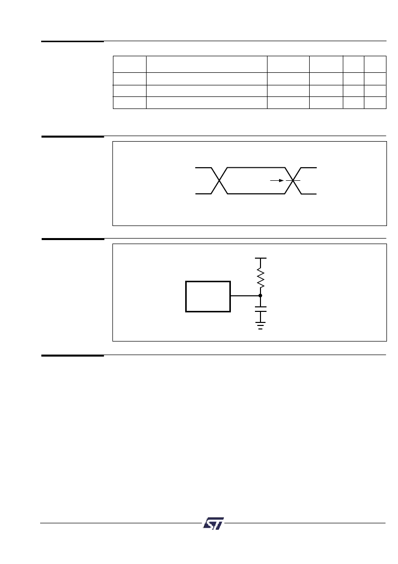
Figure 34.
AC Testing
Input/Output
Waveform
16.0
Figure 35.
AC Testing
Load Circuit
17.0
Programming
3.0V
0V
TEST POINT
1.5V
DEVICE
UNDER TEST
2.01 V
195
C
L
= 30 pF
(INCLUDING
SCOPE AND JIG
CAPACITANCE)
Upon delivery from ST, the PSD935G2 device has all bits in the PLDs and
memories in the
“
1
”
or high state. The configuration bits are in the
“
0
”
or low state. The
code, configuration, and PLDs logic are loaded through the procedure of programming.
Information for programming the device is available directly from ST. Please
contact your local sales representative. (See the last page.)
相關(guān)PDF資料 |
PDF描述 |
|---|---|
| PSD935F1V-C-90U | Configurable Memory System on a Chip for 8-Bit Microcontrollers |
| PSD935F1V-C-90UI | Configurable Memory System on a Chip for 8-Bit Microcontrollers |
| PSD935F2-70U | Configurable Memory System on a Chip for 8-Bit Microcontrollers |
| PSD935F2-70UI | Configurable Memory System on a Chip for 8-Bit Microcontrollers |
| PSD935F2-90B81 | Configurable Memory System on a Chip for 8-Bit Microcontrollers |
相關(guān)代理商/技術(shù)參數(shù) |
參數(shù)描述 |
|---|---|
| PSD935G2-90U | 功能描述:SPLD - 簡單可編程邏輯器件 TQFP-80 5V 4M 90N RoHS:否 制造商:Texas Instruments 邏輯系列:TICPAL22V10Z 大電池?cái)?shù)量:10 最大工作頻率:66 MHz 延遲時間:25 ns 工作電源電壓:4.75 V to 5.25 V 電源電流:100 uA 最大工作溫度:+ 75 C 最小工作溫度:0 C 安裝風(fēng)格:Through Hole 封裝 / 箱體:DIP-24 |
| PSD935G2V-90U | 功能描述:SPLD - 簡單可編程邏輯器件 U 511-PSD835G2V-90U RoHS:否 制造商:Texas Instruments 邏輯系列:TICPAL22V10Z 大電池?cái)?shù)量:10 最大工作頻率:66 MHz 延遲時間:25 ns 工作電源電壓:4.75 V to 5.25 V 電源電流:100 uA 最大工作溫度:+ 75 C 最小工作溫度:0 C 安裝風(fēng)格:Through Hole 封裝 / 箱體:DIP-24 |
| PSD954F2-90J | 功能描述:SPLD - 簡單可編程邏輯器件 U 511-PSD854F2-90J RoHS:否 制造商:Texas Instruments 邏輯系列:TICPAL22V10Z 大電池?cái)?shù)量:10 最大工作頻率:66 MHz 延遲時間:25 ns 工作電源電壓:4.75 V to 5.25 V 電源電流:100 uA 最大工作溫度:+ 75 C 最小工作溫度:0 C 安裝風(fēng)格:Through Hole 封裝 / 箱體:DIP-24 |
| PSD954F2-90M | 功能描述:SPLD - 簡單可編程邏輯器件 U 511-PSD854F2-90M RoHS:否 制造商:Texas Instruments 邏輯系列:TICPAL22V10Z 大電池?cái)?shù)量:10 最大工作頻率:66 MHz 延遲時間:25 ns 工作電源電壓:4.75 V to 5.25 V 電源電流:100 uA 最大工作溫度:+ 75 C 最小工作溫度:0 C 安裝風(fēng)格:Through Hole 封裝 / 箱體:DIP-24 |
| PSD954F2V-90J | 功能描述:SPLD - 簡單可編程邏輯器件 5.0V 2M 90ns RoHS:否 制造商:Texas Instruments 邏輯系列:TICPAL22V10Z 大電池?cái)?shù)量:10 最大工作頻率:66 MHz 延遲時間:25 ns 工作電源電壓:4.75 V to 5.25 V 電源電流:100 uA 最大工作溫度:+ 75 C 最小工作溫度:0 C 安裝風(fēng)格:Through Hole 封裝 / 箱體:DIP-24 |
發(fā)布緊急采購,3分鐘左右您將得到回復(fù)。