- 您現(xiàn)在的位置:買賣IC網(wǎng) > PDF目錄376299 > PSD8545V90JIT (意法半導(dǎo)體) Flash In-System Programmable ISP Peripherals For 8-bit MCUs PDF資料下載
參數(shù)資料
| 型號: | PSD8545V90JIT |
| 廠商: | 意法半導(dǎo)體 |
| 英文描述: | Flash In-System Programmable ISP Peripherals For 8-bit MCUs |
| 中文描述: | Flash在系統(tǒng)可編程ISP的外設(shè)的8位微控制器 |
| 文件頁數(shù): | 26/110頁 |
| 文件大?。?/td> | 1737K |
| 代理商: | PSD8545V90JIT |
第1頁第2頁第3頁第4頁第5頁第6頁第7頁第8頁第9頁第10頁第11頁第12頁第13頁第14頁第15頁第16頁第17頁第18頁第19頁第20頁第21頁第22頁第23頁第24頁第25頁當(dāng)前第26頁第27頁第28頁第29頁第30頁第31頁第32頁第33頁第34頁第35頁第36頁第37頁第38頁第39頁第40頁第41頁第42頁第43頁第44頁第45頁第46頁第47頁第48頁第49頁第50頁第51頁第52頁第53頁第54頁第55頁第56頁第57頁第58頁第59頁第60頁第61頁第62頁第63頁第64頁第65頁第66頁第67頁第68頁第69頁第70頁第71頁第72頁第73頁第74頁第75頁第76頁第77頁第78頁第79頁第80頁第81頁第82頁第83頁第84頁第85頁第86頁第87頁第88頁第89頁第90頁第91頁第92頁第93頁第94頁第95頁第96頁第97頁第98頁第99頁第100頁第101頁第102頁第103頁第104頁第105頁第106頁第107頁第108頁第109頁第110頁
PSD813F2, PSD833F2, PSD834F2, PSD853F2, PSD854F2
26/110
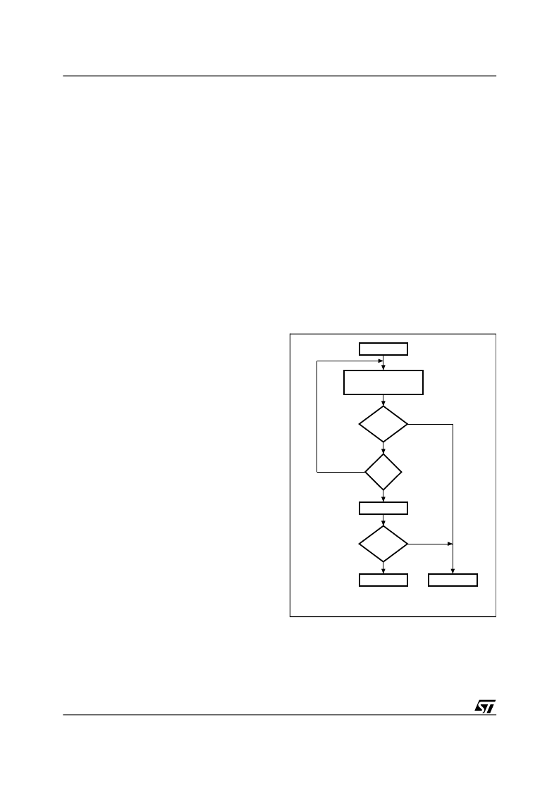
Data Toggle
Checking the Toggle Flag Bit (DQ6) is a method of
determining whether a Program or Erase cycle is
in progress or has completed. Figure
8
shows the
Data Toggle algorithm.
When the MCU issues a Program instruction, the
embedded algorithm within the PSD begins. The
MCU then reads the location of the byte to be pro-
grammed in Flash memory to check status. The
Toggle Flag Bit (DQ6) of this location toggles each
time the MCU reads this location until the embed-
ded algorithm is complete. The MCU continues to
read this location, checking the Toggle Flag Bit
(DQ6) and monitoring the Error Flag Bit (DQ5).
When the Toggle Flag Bit (DQ6) stops toggling
(two consecutive reads yield the same value), and
the Error Flag Bit (DQ5) remains ’0,’ the embed-
ded algorithm is complete. If the Error Flag Bit
(DQ5) is '1,' the MCU should test the Toggle Flag
Bit (DQ6) again, since the Toggle Flag Bit (DQ6)
may have changed simultaneously with the Error
Flag Bit (DQ5, see Figure
8
).
The Error Flag Bit (DQ5) is set if either an internal
time-out occurred while the embedded algorithm
attempted to program the byte, or if the MCU at-
tempted to program a '1' to a bit that was not
erased (not erased is logic '0').
It is suggested (as with all Flash memories) to read
the location again after the embedded program-
ming algorithm has completed, to compare the
byte that was written to Flash memory with the
byte that was intended to be written.
When using the Data Toggle method after an
Erase cycle, Figure
8
still applies. the Toggle Flag
Bit (DQ6) toggles until the Erase cycle is complete.
A '1' on the Error Flag Bit (DQ5) indicates a time-
out condition on the Erase cycle; a '0' indicates no
error. The MCU can read any location within the
sector being erased to get the Toggle Flag Bit
(DQ6) and the Error Flag Bit (DQ5).
PSDsoft Express generates ANSI C code func-
tions which implement these Data Toggling algo-
rithms.
Unlock Bypass (PSD833F2x, PSD834F2x,
PSD853F2x, PSD854F2x)
The Unlock Bypass instructions allow the system
to program bytes to the Flash memories faster
than using the standard Program instruction. The
Unlock Bypass mode is entered by first initiating
two Unlock cycles. This is followed by a third
WRITE cycle containing the Unlock Bypass code,
20h (as shown in
Table 9., page 21
).
The Flash memory then enters the Unlock Bypass
mode. A two-cycle Unlock Bypass Program in-
struction is all that is required to program in this
mode. The first cycle in this instruction contains
the Unlock Bypass Program code, A0h. The sec-
ond cycle contains the program address and data.
Additional data is programmed in the same man-
ner. These instructions dispense with the initial
two Unlock cycles required in the standard Pro-
gram instruction, resulting in faster total Flash
memory programming.
During the Unlock Bypass mode, only the Unlock
Bypass Program and Unlock Bypass Reset Flash
instructions are valid.
To exit the Unlock Bypass mode, the system must
issue the two-cycle Unlock Bypass Reset Flash in-
struction. The first cycle must contain the data
90h; the second cycle the data 00h. Addresses are
Don’t Care for both cycles. The Flash memory
then returns to READ Mode.
Figure 8. Data Toggle Flowchart
READ
DQ5 & DQ6
START
READ DQ6
FAIL
PASS
AI01370B
D=
TOGGLE
NO
NO
YES
YES
DQ5
= 1
NO
YES
D=
TOGGLE
相關(guān)PDF資料 |
PDF描述 |
|---|---|
| PSD9545V90JIT | Flash In-System Programmable ISP Peripherals For 8-bit MCUs |
| PSD9135V90JT | Flash In-System Programmable ISP Peripherals For 8-bit MCUs |
| PSD8335V90JT | Flash In-System Programmable ISP Peripherals For 8-bit MCUs |
| PSD9335V90JT | Flash In-System Programmable ISP Peripherals For 8-bit MCUs |
| PSD8535V90JT | Flash In-System Programmable ISP Peripherals For 8-bit MCUs |
相關(guān)代理商/技術(shù)參數(shù) |
參數(shù)描述 |
|---|---|
| PSD854F2-15J | 制造商:STMicroelectronics 功能描述:4556DIE2HR - Trays |
| PSD854F2-70J | 功能描述:CPLD - 復(fù)雜可編程邏輯器件 5.0V 2M 70ns RoHS:否 制造商:Lattice 系列: 存儲類型:EEPROM 大電池?cái)?shù)量:128 最大工作頻率:333 MHz 延遲時間:2.7 ns 可編程輸入/輸出端數(shù)量:64 工作電源電壓:3.3 V 最大工作溫度:+ 90 C 最小工作溫度:0 C 封裝 / 箱體:TQFP-100 |
| PSD854F2-70M | 功能描述:CPLD - 復(fù)雜可編程邏輯器件 5.0V 2M 70ns RoHS:否 制造商:Lattice 系列: 存儲類型:EEPROM 大電池?cái)?shù)量:128 最大工作頻率:333 MHz 延遲時間:2.7 ns 可編程輸入/輸出端數(shù)量:64 工作電源電壓:3.3 V 最大工作溫度:+ 90 C 最小工作溫度:0 C 封裝 / 箱體:TQFP-100 |
| PSD854F2-90J | 功能描述:CPLD - 復(fù)雜可編程邏輯器件 5.0V 2M 90ns RoHS:否 制造商:Lattice 系列: 存儲類型:EEPROM 大電池?cái)?shù)量:128 最大工作頻率:333 MHz 延遲時間:2.7 ns 可編程輸入/輸出端數(shù)量:64 工作電源電壓:3.3 V 最大工作溫度:+ 90 C 最小工作溫度:0 C 封裝 / 箱體:TQFP-100 |
| PSD854F2-90JI | 功能描述:CPLD - 復(fù)雜可編程邏輯器件 5.0V 2M 90ns RoHS:否 制造商:Lattice 系列: 存儲類型:EEPROM 大電池?cái)?shù)量:128 最大工作頻率:333 MHz 延遲時間:2.7 ns 可編程輸入/輸出端數(shù)量:64 工作電源電壓:3.3 V 最大工作溫度:+ 90 C 最小工作溫度:0 C 封裝 / 箱體:TQFP-100 |
發(fā)布緊急采購,3分鐘左右您將得到回復(fù)。