- 您現(xiàn)在的位置:買賣IC網(wǎng) > PDF目錄368238 > PSD835F2V-A-15B81I (意法半導(dǎo)體) Configurable Memory System on a Chip for 8-Bit Microcontrollers PDF資料下載
參數(shù)資料
| 型號: | PSD835F2V-A-15B81I |
| 廠商: | 意法半導(dǎo)體 |
| 英文描述: | Configurable Memory System on a Chip for 8-Bit Microcontrollers |
| 中文描述: | 在8片位微控制器可配置存儲系統(tǒng) |
| 文件頁數(shù): | 43/110頁 |
| 文件大?。?/td> | 570K |
| 代理商: | PSD835F2V-A-15B81I |
第1頁第2頁第3頁第4頁第5頁第6頁第7頁第8頁第9頁第10頁第11頁第12頁第13頁第14頁第15頁第16頁第17頁第18頁第19頁第20頁第21頁第22頁第23頁第24頁第25頁第26頁第27頁第28頁第29頁第30頁第31頁第32頁第33頁第34頁第35頁第36頁第37頁第38頁第39頁第40頁第41頁第42頁當(dāng)前第43頁第44頁第45頁第46頁第47頁第48頁第49頁第50頁第51頁第52頁第53頁第54頁第55頁第56頁第57頁第58頁第59頁第60頁第61頁第62頁第63頁第64頁第65頁第66頁第67頁第68頁第69頁第70頁第71頁第72頁第73頁第74頁第75頁第76頁第77頁第78頁第79頁第80頁第81頁第82頁第83頁第84頁第85頁第86頁第87頁第88頁第89頁第90頁第91頁第92頁第93頁第94頁第95頁第96頁第97頁第98頁第99頁第100頁第101頁第102頁第103頁第104頁第105頁第106頁第107頁第108頁第109頁第110頁
PSD8XX Family
PSD835G2
42
MASTER
MCU
MCU-RD
MCU-RD
MCU-WR
SLAVE
–
WR
SLAVE
–
CS
MCU-WR
D[7:0]
D[7:0]
CPLD
D
Q
Q
D
PORT A
DATA OUT
REGISTER
PORT A
INPUT
MICRO
CELL
PORT A
SLAVE
–
READ
SLAVE
MCU
RD
WR
PSD835G2
Figure 15. Handshaking Communication Using Input Micro
Cells
The
PSD835G2
Functional
Blocks
(cont.)
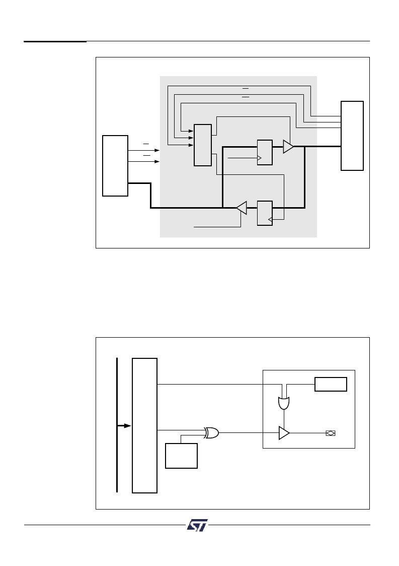
9.2.2.7 External Chip Select
The CPLD also provides eight chip select outputs that can be used to select external
devices. The chip selects can be routed to either Port C or Port F, depending on the pin
declaration in the PSDsoft. Each chip select (ECS0-7) consists of one product term that can
be configured active high or low.
The output enable of the pin is controlled by either the output enable product term or the
Direction Register. (See Figure 16).
CPLD
AND
ARRAY
ECS PT
P
PORT C OR PORT F
ECS
TO PORT C OR F
ENABLE (.OE) PT
POLARITY
BIT
DIRECTION
REGISTER
PORT PIN
Figure 16. External Chip Select
發(fā)布緊急采購,3分鐘左右您將得到回復(fù)。