- 您現(xiàn)在的位置:買賣IC網(wǎng) > PDF目錄224799 > PSD4235G2V-B-15JI (意法半導(dǎo)體) Flash In-System-Programmable Peripherals for 16-Bit MCUs PDF資料下載
參數(shù)資料
| 型號: | PSD4235G2V-B-15JI |
| 廠商: | 意法半導(dǎo)體 |
| 英文描述: | Flash In-System-Programmable Peripherals for 16-Bit MCUs |
| 中文描述: | Flash在系統(tǒng)可編程外設(shè)的16位微控制器 |
| 文件頁數(shù): | 47/93頁 |
| 文件大小: | 503K |
| 代理商: | PSD4235G2V-B-15JI |
第1頁第2頁第3頁第4頁第5頁第6頁第7頁第8頁第9頁第10頁第11頁第12頁第13頁第14頁第15頁第16頁第17頁第18頁第19頁第20頁第21頁第22頁第23頁第24頁第25頁第26頁第27頁第28頁第29頁第30頁第31頁第32頁第33頁第34頁第35頁第36頁第37頁第38頁第39頁第40頁第41頁第42頁第43頁第44頁第45頁第46頁當(dāng)前第47頁第48頁第49頁第50頁第51頁第52頁第53頁第54頁第55頁第56頁第57頁第58頁第59頁第60頁第61頁第62頁第63頁第64頁第65頁第66頁第67頁第68頁第69頁第70頁第71頁第72頁第73頁第74頁第75頁第76頁第77頁第78頁第79頁第80頁第81頁第82頁第83頁第84頁第85頁第86頁第87頁第88頁第89頁第90頁第91頁第92頁第93頁
PSD4000 Series
Preliminary Information
48
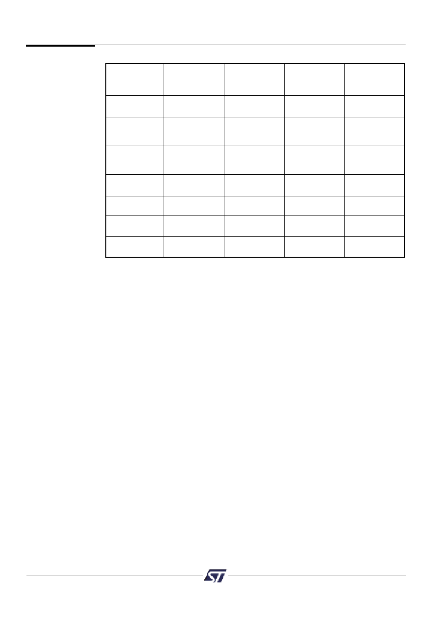
Control
Direction
VM
Defined In
Register
Mode
PSDsoft
Setting
Declare
0
1 = output,
MCU I/O
pins only
(Note 1)
0 = input
NA
Declare pins
PLD I/O
and logic or chip
NA
select equations
Data Port
Selected for
(Port F, G)
MCU with
NA
non-mux bus
Address Out
Declare
11
NA
(Port E, F, G)
pins only
Address In
Declare pins
(Port A,B,C,D,F)
NA
JTAG ISP
Declare pins
NA
only
MCU Reset
Specify pin
NA
Mode
logic level
Table 17. Port Operating Mode Settings
*NA = Not Applicable
NOTE: 1. Control Register setting is not applicable to Ports A, B and C.
9.4.2.1 MCU I/O Mode
In the MCU I/O Mode, the microcontroller uses the PSD4000 ports to expand its own
I/O ports. By setting up the CSIOP space, the ports on the PSD4000 are mapped into the
microcontroller address space. The addresses of the ports are listed in Table 6.
A port pin can be put into MCU I/O mode by writing a ‘0’ to the corresponding bit in the
Control Register (Port E, F and G). The MCU I/O direction may be changed by writing
to the corresponding bit in the Direction Register. See the subsection on the Direction
Register in the “Port Registers” section. When the pin is configured as an output, the
content of the Data Out Register drives the pin. When configured as an input, the
microcontroller can read the port input through the Data In buffer. See Figure 20.
Ports A, B and C do not have Control Registers, and are in MCU I/O mode by default.
They can be used for PLD I/O if they are specified in PSDsoft.
9.4.2.2 PLD I/O Mode
The PLD I/O Mode uses a port as an input to the CPLD’s Input Micro
Cells, and/or
as an output from the GPLD. The corresponding bit in the Direction Register must not be
set to ‘1’ if the pin is defined as a PLD input pin in PSDsoft. The PLD I/O Mode is specified
in PSDsoft by declaring the port pins, and then specifying an equation in PSDsoft.
The
PSD4000
Functional
Blocks
(cont.)
發(fā)布緊急采購,3分鐘左右您將得到回復(fù)。