- 您現(xiàn)在的位置:買賣IC網(wǎng) > PDF目錄368227 > PSD4235G2-B-70JI (意法半導(dǎo)體) Solid Tantalum Chip Capacitors / T491 Series - Precision Molded Chip; Capacitance [nom]: 0.47uF; Working Voltage (Vdc)[max]: 35V; Capacitance Tolerance: +/-10%; Dielectric: Tantalum, Solid; Lead Style: Surface-Mount Chip; Lead Dimensions: 3216-18; Termination: 100% Tin (Sn); Body Dimensions: 3.2mm x 1.6mm x 1.6mm; Temperature Range: -55C to +125C; Container: Tape & Reel; Qty per Container: 2,000 PDF資料下載
參數(shù)資料
| 型號(hào): | PSD4235G2-B-70JI |
| 廠商: | 意法半導(dǎo)體 |
| 英文描述: | Solid Tantalum Chip Capacitors / T491 Series - Precision Molded Chip; Capacitance [nom]: 0.47uF; Working Voltage (Vdc)[max]: 35V; Capacitance Tolerance: +/-10%; Dielectric: Tantalum, Solid; Lead Style: Surface-Mount Chip; Lead Dimensions: 3216-18; Termination: 100% Tin (Sn); Body Dimensions: 3.2mm x 1.6mm x 1.6mm; Temperature Range: -55C to +125C; Container: Tape & Reel; Qty per Container: 2,000 |
| 中文描述: | Flash在系統(tǒng)可編程外設(shè)的16位微控制器 |
| 文件頁(yè)數(shù): | 33/89頁(yè) |
| 文件大小: | 703K |
| 代理商: | PSD4235G2-B-70JI |
第1頁(yè)第2頁(yè)第3頁(yè)第4頁(yè)第5頁(yè)第6頁(yè)第7頁(yè)第8頁(yè)第9頁(yè)第10頁(yè)第11頁(yè)第12頁(yè)第13頁(yè)第14頁(yè)第15頁(yè)第16頁(yè)第17頁(yè)第18頁(yè)第19頁(yè)第20頁(yè)第21頁(yè)第22頁(yè)第23頁(yè)第24頁(yè)第25頁(yè)第26頁(yè)第27頁(yè)第28頁(yè)第29頁(yè)第30頁(yè)第31頁(yè)第32頁(yè)當(dāng)前第33頁(yè)第34頁(yè)第35頁(yè)第36頁(yè)第37頁(yè)第38頁(yè)第39頁(yè)第40頁(yè)第41頁(yè)第42頁(yè)第43頁(yè)第44頁(yè)第45頁(yè)第46頁(yè)第47頁(yè)第48頁(yè)第49頁(yè)第50頁(yè)第51頁(yè)第52頁(yè)第53頁(yè)第54頁(yè)第55頁(yè)第56頁(yè)第57頁(yè)第58頁(yè)第59頁(yè)第60頁(yè)第61頁(yè)第62頁(yè)第63頁(yè)第64頁(yè)第65頁(yè)第66頁(yè)第67頁(yè)第68頁(yè)第69頁(yè)第70頁(yè)第71頁(yè)第72頁(yè)第73頁(yè)第74頁(yè)第75頁(yè)第76頁(yè)第77頁(yè)第78頁(yè)第79頁(yè)第80頁(yè)第81頁(yè)第82頁(yè)第83頁(yè)第84頁(yè)第85頁(yè)第86頁(yè)第87頁(yè)第88頁(yè)第89頁(yè)
33/89
PSD4235G2
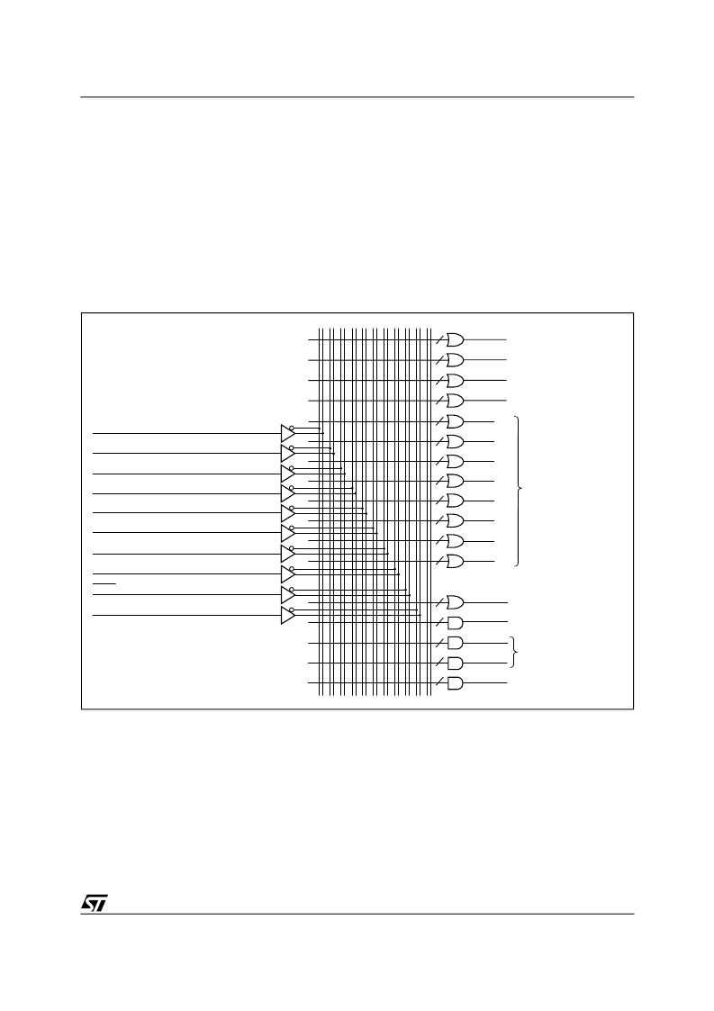
DECODE PLD (DPLD)
The DPLD, shown in Figure 13, is used for decod-
ing the address for internal and external compo-
nents. The DPLD can be used to generate the
following decode signals:
I
8 Sector Select (FS0-FS7) signals for the
primary Flash memory (three product terms
each)
I
4 Sector Select (CSBOOT0-CSBOOT3) signals
for the secondary Flash memory (three product
terms each)
I
1 internal SRAM Select (RS0) signal (three
product terms)
I
1 internal CSIOP Select (PSD Configuration
Register) signal
I
1 JTAG Select signal (enables JTAG-ISP on
Port E)
I
2 internal Peripheral Select signals
(Peripheral I/O mode).
Figure 13. DPLD Logic Array
Note: 1. The address inputs are A19-A4 when in 80C51XA mode
2. Additional address lines can be brought ino the PSD via Port A, B, C, D, or F.
(INPUTS)
(32)
(8)
(16)
(1)
PDN (APD OUTPUT)
I/O PORTS (PORT A,B,F)
(8)
PGR0 -PGR7
(8)
MCELLAB.FB [7:0] (FEEDBACKS)
MCELLBC.FB [7:0] (FEEDBACKS)
A[15:0]
*
(4)
(3)
PD[3:0] (ALE,CLKIN,CSI)
CNTRL[2:0] (READ/WRITE CONTROL SIGNALS)
(1)
(1)
RESET
RD_BSY
RS0
CSIOP
PSEL0
PSEL1
8 PRIMARY FLASH
MEMORY SECTOR SELECTS
SRAM SELECT
I/O DECODER
SELECT
PERIPHERAL I/O MODE
SELECT
CSBOOT 0
CSBOOT 1
CSBOOT 2
CSBOOT 3
FS0
FS7
3
3
3
3
3
3
3
3
3
3
3
3
3
JTAGSEL
AI05738
FS1
FS2
FS3
FS6
FS5
FS4
1
1
1
1
相關(guān)PDF資料 |
PDF描述 |
|---|---|
| PSD4235G2-C-70B81 | Flash In-System-Programmable Peripherals for 16-Bit MCUs |
| PSD4235G2-C-70B81I | Flash In-System-Programmable Peripherals for 16-Bit MCUs |
| PSD4235G2-C-70J | Flash In-System-Programmable Peripherals for 16-Bit MCUs |
| PSD4235G2-C-70JI | Flash In-System-Programmable Peripherals for 16-Bit MCUs |
| PSD4235G2-C-70M | CAP 4.7UF 4V 20% TANT SMD-3216-18 TR-13-PL GOLD |
相關(guān)代理商/技術(shù)參數(shù) |
參數(shù)描述 |
|---|---|
| PSD4235G2V-12UI | 功能描述:CPLD - 復(fù)雜可編程邏輯器件 3.3V 4M 120ns RoHS:否 制造商:Lattice 系列: 存儲(chǔ)類型:EEPROM 大電池?cái)?shù)量:128 最大工作頻率:333 MHz 延遲時(shí)間:2.7 ns 可編程輸入/輸出端數(shù)量:64 工作電源電壓:3.3 V 最大工作溫度:+ 90 C 最小工作溫度:0 C 封裝 / 箱體:TQFP-100 |
| PSD4235G2V-90U | 功能描述:CPLD - 復(fù)雜可編程邏輯器件 3.3V 4M 90ns RoHS:否 制造商:Lattice 系列: 存儲(chǔ)類型:EEPROM 大電池?cái)?shù)量:128 最大工作頻率:333 MHz 延遲時(shí)間:2.7 ns 可編程輸入/輸出端數(shù)量:64 工作電源電壓:3.3 V 最大工作溫度:+ 90 C 最小工作溫度:0 C 封裝 / 箱體:TQFP-100 |
| PSD4256G6V-10UI | 功能描述:CPLD - 復(fù)雜可編程邏輯器件 3.3V 8M 100ns RoHS:否 制造商:Lattice 系列: 存儲(chǔ)類型:EEPROM 大電池?cái)?shù)量:128 最大工作頻率:333 MHz 延遲時(shí)間:2.7 ns 可編程輸入/輸出端數(shù)量:64 工作電源電壓:3.3 V 最大工作溫度:+ 90 C 最小工作溫度:0 C 封裝 / 箱體:TQFP-100 |
| PSD4-36 | 制造商:Tamura Corporation of America 功能描述: |
| PSD-45 | 制造商:MEANWELL 制造商全稱:Mean Well Enterprises Co., Ltd. 功能描述:45W DC-DC Single Output Switching Power Supply |
發(fā)布緊急采購(gòu),3分鐘左右您將得到回復(fù)。