- 您現(xiàn)在的位置:買賣IC網(wǎng) > PDF目錄98060 > PS395CNB (PERICOM SEMICONDUCTOR CORP) OCTAL 1-CHANNEL, SGL POLE SGL THROW SWITCH, PDIP24 PDF資料下載
參數(shù)資料
| 型號(hào): | PS395CNB |
| 廠商: | PERICOM SEMICONDUCTOR CORP |
| 元件分類: | 多路復(fù)用及模擬開關(guān) |
| 英文描述: | OCTAL 1-CHANNEL, SGL POLE SGL THROW SWITCH, PDIP24 |
| 封裝: | PLASTIC, DIP-24 |
| 文件頁(yè)數(shù): | 1/13頁(yè) |
| 文件大?。?/td> | 410K |
| 代理商: | PS395CNB |
當(dāng)前第1頁(yè)第2頁(yè)第3頁(yè)第4頁(yè)第5頁(yè)第6頁(yè)第7頁(yè)第8頁(yè)第9頁(yè)第10頁(yè)第11頁(yè)第12頁(yè)第13頁(yè)
1
PS8462
02/22/00
Features
Low On-Resistance (100 typ.)
Minimizes Distortion and Error Voltages
Single Supply Operation (±2.7V to ±8V)
Improved Second Source for MAX395
SPI/QSI, Microwire-Compatible Serial Interface
Split-Supply Operation (+3V to +8V)
On-Resistance Flatness: 10 Max.
On-Resistance Matching Between Channels: 5 Max.
TTL/CMOS Logic Compatible (w/+5V or ±5V supplies)
Fast Switching Speed
Break-Before-Make action eliminates momentary crosstalk
Rail-to-Rail Analog Signal Range
Low Power Consumption
Narrow SOIC and QSOP Packages Minimize Board Area
Asynchonous Reset (RS) Input
Applications
Data Acquisition Systems
Audio Switching and Routing
Test Equipment
PBX, PABX
Telecommunication Systems
Battery-Powered Systems
Description
The PS395 eight-channel, serially controlled, single-pole/single-
throw (SPST) analog switch offers eight separately controlled
switches that conduct equally well in either direction. ON-resis-
tance (100 max.) is matched between switches to 5 max. and is
flat (10 max.) over the specified signal range.
These CMOS devices can operate continuously with dual power
supplies ranging from ±2.7V to ±8V or a single supply between
+2.7V and +16V. Each switch can handle rail-to-rail analog signals.
The off leakage current is only 0.1nA at +25°C or 5nA at +85°C.
Upon power-up, all switches are off, and the internal shift registers
are reset to zero. The PS395 is electrically equivalent to two PS391
quad switches controlled by a serial interface, and is pin compat-
ible with the PS335.
The serial interface is compatible with SPI/QSPI and
Microwire. Functioning as a shift register, it allows data (at DIN)
to be clocked-in synchronously with the rising edge of clock
(SCLK). The shift registers output (DOUT) enables several PS395s
to be daisy chained.
All digital inputs have 0.8V to 2.4V logic thresholds, ensuring both
TTL- and CMOS-logic compatibility when using ±5V supplies or a
single +5V supply.
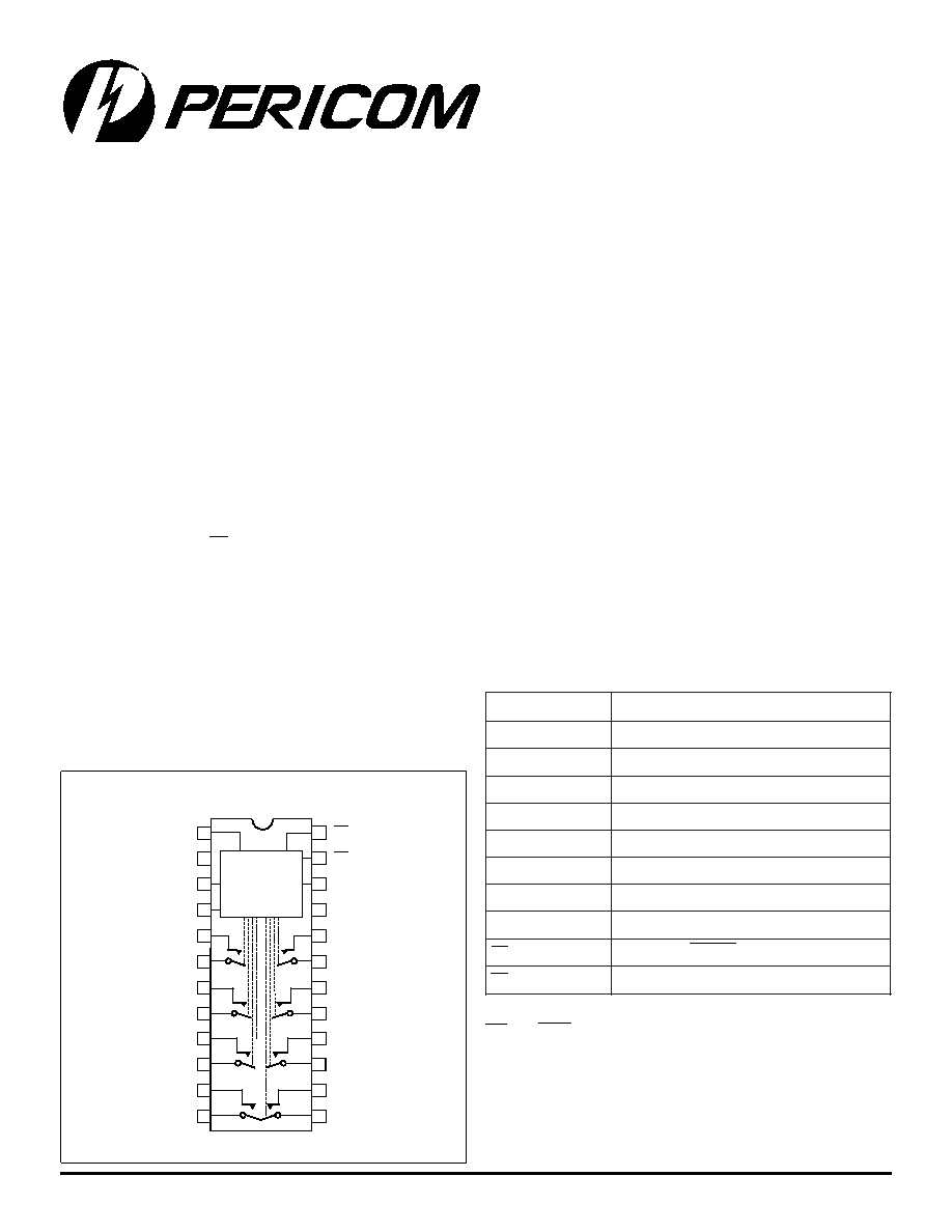
Pin Configurations
e
m
a
Nn
o
it
c
n
u
F
K
L
Ct
u
p
n
I
l
a
ti
g
i
D
k
c
o
l
C
l
ai
r
e
S
+
Vt
u
p
n
I
e
g
a
tl
o
V
y
l
p
u
S
g
o
l
a
n
A
e
v
it
i
s
o
P
A
T
A
D
N
I
t
u
p
n
I
l
a
ti
g
i
D
a
t
a
D
l
ai
r
e
S
D
N
Gd
n
u
o
r
G
O
N 0 O
N
7
0
s
e
h
c
ti
w
S
g
o
l
a
n
A
n
e
p
O
y
ll
a
m
r
o
N
M
O
C
0
M
O
C
7
0
s
e
h
c
ti
w
S
g
o
l
a
n
A
n
o
m
o
C
Vt
u
p
n
I
e
g
a
tl
o
V
y
l
p
u
S
g
o
l
a
n
A
e
v
it
a
g
e
N
A
T
A
D
T
U
O
t
u
p
t
u
O
l
a
ti
g
i
D
a
t
a
D
l
ai
r
e
S
Rt
u
p
n
I
t
e
s
e
R
)
T
E
S
E
R
(
S
Ct
u
p
n
I
l
a
ti
g
i
D
t
c
el
e
S
-
p
i
h
C
Pin Description
Note:
NO and COM pins are identical and interchangeble. Either may
be considered as an input or an output; signals pass equally
well in either direction.
PS395
Precision 8-Ch. 17V, SPST Switch
w/8-Bit Serial Decoded Control
12345678901234567890123456789012123456789012345678901234567890121234567890123456789012345678901212345678901234567890123456789012123456789012
16
15
14
13
8
1
2
3
4
5
6
7
9
10
11
12
17
24
23
22
21
20
19
18
CLK
V+
DATAIN
GND
NO0
COM0
NO1
COM1
NO2
COM2
NO3
COM3
DIP/SO
EN
RS
DATAOUT
V–
NO7
COM7
NO6
COM6
NO5
COM5
NO4
COM4
8-Bit
Decoding
Logic
SPI & QSPI are trademarks of Motorola, Inc. Microwire is a trademark
of National Semiconductor Corporation
Top View
PS395
相關(guān)PDF資料 |
PDF描述 |
|---|---|
| PS395ENG | OCTAL 1-CHANNEL, SGL POLE SGL THROW SWITCH, PDIP24 |
| PS395CWG | OCTAL 1-CHANNEL, SGL POLE SGL THROW SWITCH, PDSO24 |
| PS395EWG | OCTAL 1-CHANNEL, SGL POLE SGL THROW SWITCH, PDSO24 |
| PS395CPG | OCTAL 1-CHANNEL, SGL POLE SGL THROW SWITCH, PDIP24 |
| PS399EEE | 4-CHANNEL, DIFFERENTIAL MULTIPLEXER, PDSO16 |
相關(guān)代理商/技術(shù)參數(shù) |
參數(shù)描述 |
|---|---|
| PS395CWG | 制造商:未知廠家 制造商全稱:未知廠家 功能描述:ANALOG SWITCH|OCTAL|SPST|CMOS|SOP|24PIN|PLASTIC |
| PS395ENG | 制造商:未知廠家 制造商全稱:未知廠家 功能描述:ANALOG SWITCH|OCTAL|SPST|CMOS|DIP|24PIN|PLASTIC |
| PS395EWG | 制造商:未知廠家 制造商全稱:未知廠家 功能描述:ANALOG SWITCH|OCTAL|SPST|CMOS|SOP|24PIN|PLASTIC |
| PS396 | 制造商:PERICOM 制造商全稱:Pericom Semiconductor Corporation 功能描述:Precision, 16-Channel 17V Analog Multiplexer |
| PS396CAI | 制造商:PERICOM 制造商全稱:Pericom Semiconductor Corporation 功能描述:Precision, 16-Channel 17V Analog Multiplexer |
發(fā)布緊急采購(gòu),3分鐘左右您將得到回復(fù)。