- 您現(xiàn)在的位置:買(mǎi)賣(mài)IC網(wǎng) > PDF目錄65942 > PKF4928API (ERICSSON POWER MODULES AB) 2-OUTPUT 9.43 W DC-DC REG PWR SUPPLY MODULE PDF資料下載
參數(shù)資料
| 型號(hào): | PKF4928API |
| 廠(chǎng)商: | ERICSSON POWER MODULES AB |
| 元件分類(lèi): | 電源模塊 |
| 英文描述: | 2-OUTPUT 9.43 W DC-DC REG PWR SUPPLY MODULE |
| 封裝: | 8 MM HEIGHT, POWER, MODULE-18 |
| 文件頁(yè)數(shù): | 7/8頁(yè) |
| 文件大?。?/td> | 520K |
| 代理商: | PKF4928API |
7
EN/LZT 146 99 R1A Ericsson Microelectronics AB, June 2001
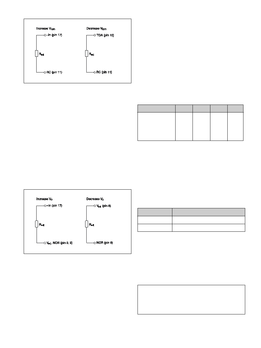
Output Voltage Adjust (Vadj)
Output voltage, VO, can be adjusted by using an external resistor
or other external circuitry. If other circuitry is used, the slew rate
has to be limited to maximum 5 V/ms. If pins 8 and 9 are not
connected together the output will decrease to a low value. To
increase VO a resistor should be connected between pin 8/9 and 17,
and to decrease VO a resistor should be connected between pin 8
and 9 (see fig. 3).
To increase output voltage:
Rounom= 3.95×(4.21-VO)/(VO-VI) k
W
VI is the initial output voltage when pin 8 and 9 are connected,
VO is the desired output voltage.
To decrease output voltage:
Rodnom=17.6×(VI-VO)/(VO-1.74) k
W
VI is the initial output voltage when pin 8 and 9 are connected,
VO is the desired output voltage.
Figure 3
Current Limiting Protection (Ilim)
The output power is limited at loads above the output current
limiting threshold (Ilim), specified as a minimum value.
Capacitive Load
The PKF series has no maximum limit for capacitive load on the
output. The power module may operate in current limiting mode
during start-up, affecting the ramp-up and the start-up time. For
optimum start performance we recommend maximum 100
mF/A of
IO. Connect capacitors at the point of load for best performance.
Input and Output Impedance
Both the source impedance of the power feeding and the load
impedance will interact with the impedance of the DC/DC power
module.
It is most important to have the ratio between L and C as low as
possible, i.e. a low characteristic impedance, both at the input and
output, as the power modules have a low energy storage capability.
Use an electrolytic capacitor across the input if the source induct-
ance is higher than 10
mH. Their equivalent series resistance to-
gether with the capacitance acts as a lossless damping filter.
Suitable capacitor values are in the range 10–100
mF.
Parallel Operation
Paralleling of several converters is easily accomplished by direct
connection of the output voltage terminal pins. The load regula-
tion characteristic is specifically designed for optimum paralleling
performance. Load sharing between converters will be within
±10%. It is recommended not to exceed PO = n × 0.9 × POmax,
where POmax is the maximum converter output power and n the
number of paralleled converters, to prevent overloading any of the
converters and thereby decreasing the reliability performance.
Synchronization (Sync)
It is possible to synchronize the switching frequency to an external
symmetrical clock signal. The input can be driven by an TTL-
compatible output and referenced to the input pin 17.
Information given in this data sheet is believed to be accurate and reliable. No
responsibility is assumed for the consequences of its use nor for any infringement
of patents or other rights of third parties which may result from its use.
No license is granted by implication or otherwise under any patent or patent rights of
Ericsson Microelectronics. These products are sold only according to Ericsson
Microelectronics’ general conditions of sale, unless otherwise confirmed in writing.
Specifications subject to change without notice.
Order Info
Surface mount
PKF 4928A SI
Through hole
PKF 4928A PI
Version
Part No.
Figure 2
Characteristics
min
typ
max
unit
High level
2.2
6.5
V
Threshold level*)
1.2
1.7
2.2
V
Low level
0
0.4
V
Sink current
1.5
mA
Sync. frequency
520
688
kHz
*)
Rise time <10ns
相關(guān)PDF資料 |
PDF描述 |
|---|---|
| PKF4928ASI | 2-OUTPUT 9.43 W DC-DC REG PWR SUPPLY MODULE |
| PKJ4110BPIPT | 1-OUTPUT 132 W DC-DC REG PWR SUPPLY MODULE |
| PKJ4119BPITLA | 1-OUTPUT 100 W DC-DC REG PWR SUPPLY MODULE |
| PKJ4718BPITLA | 1-OUTPUT 72 W DC-DC REG PWR SUPPLY MODULE |
| PKJ4119BPIPT | 1-OUTPUT 100 W DC-DC REG PWR SUPPLY MODULE |
相關(guān)代理商/技術(shù)參數(shù) |
參數(shù)描述 |
|---|---|
| PKF50B1/4 | 制造商:TE Connectivity 功能描述: |
| PKF50B1/8 | 功能描述:旋鈕和轉(zhuǎn)盤(pán) QUARATE0.669"W/SKIRT SWITCH KNOB RoHS:否 制造商:Davies Molding 材料:Phenolic 設(shè)計(jì):Set Screw 軸尺寸:0.25 in 直徑:3/4 in 顏色:Black 指示器型式:Line |
| PKF5510PI | 制造商:ERICSSON 制造商全稱(chēng):Ericsson 功能描述:5-6 W DC/DC Power Modules Wide Input Series |
| PKF5510SI | 制造商:ERICSSON 制造商全稱(chēng):Ericsson 功能描述:5-6 W DC/DC Power Modules Wide Input Series |
| PKF5611PI | 制造商:ERICSSON 制造商全稱(chēng):Ericsson 功能描述:5-6 W DC/DC Power Modules Wide Input Series |
發(fā)布緊急采購(gòu),3分鐘左右您將得到回復(fù)。