- 您現(xiàn)在的位置:買(mǎi)賣(mài)IC網(wǎng) > PDF目錄299771 > PIC16C925/L 8-BIT, OTPROM, 20 MHz, RISC MICROCONTROLLER, PQCC68 PDF資料下載
參數(shù)資料
| 型號(hào): | PIC16C925/L |
| 元件分類(lèi): | 微控制器/微處理器 |
| 英文描述: | 8-BIT, OTPROM, 20 MHz, RISC MICROCONTROLLER, PQCC68 |
| 封裝: | PLASTIC, LCC-68 |
| 文件頁(yè)數(shù): | 120/183頁(yè) |
| 文件大小: | 3233K |
| 代理商: | PIC16C925/L |
第1頁(yè)第2頁(yè)第3頁(yè)第4頁(yè)第5頁(yè)第6頁(yè)第7頁(yè)第8頁(yè)第9頁(yè)第10頁(yè)第11頁(yè)第12頁(yè)第13頁(yè)第14頁(yè)第15頁(yè)第16頁(yè)第17頁(yè)第18頁(yè)第19頁(yè)第20頁(yè)第21頁(yè)第22頁(yè)第23頁(yè)第24頁(yè)第25頁(yè)第26頁(yè)第27頁(yè)第28頁(yè)第29頁(yè)第30頁(yè)第31頁(yè)第32頁(yè)第33頁(yè)第34頁(yè)第35頁(yè)第36頁(yè)第37頁(yè)第38頁(yè)第39頁(yè)第40頁(yè)第41頁(yè)第42頁(yè)第43頁(yè)第44頁(yè)第45頁(yè)第46頁(yè)第47頁(yè)第48頁(yè)第49頁(yè)第50頁(yè)第51頁(yè)第52頁(yè)第53頁(yè)第54頁(yè)第55頁(yè)第56頁(yè)第57頁(yè)第58頁(yè)第59頁(yè)第60頁(yè)第61頁(yè)第62頁(yè)第63頁(yè)第64頁(yè)第65頁(yè)第66頁(yè)第67頁(yè)第68頁(yè)第69頁(yè)第70頁(yè)第71頁(yè)第72頁(yè)第73頁(yè)第74頁(yè)第75頁(yè)第76頁(yè)第77頁(yè)第78頁(yè)第79頁(yè)第80頁(yè)第81頁(yè)第82頁(yè)第83頁(yè)第84頁(yè)第85頁(yè)第86頁(yè)第87頁(yè)第88頁(yè)第89頁(yè)第90頁(yè)第91頁(yè)第92頁(yè)第93頁(yè)第94頁(yè)第95頁(yè)第96頁(yè)第97頁(yè)第98頁(yè)第99頁(yè)第100頁(yè)第101頁(yè)第102頁(yè)第103頁(yè)第104頁(yè)第105頁(yè)第106頁(yè)第107頁(yè)第108頁(yè)第109頁(yè)第110頁(yè)第111頁(yè)第112頁(yè)第113頁(yè)第114頁(yè)第115頁(yè)第116頁(yè)第117頁(yè)第118頁(yè)第119頁(yè)當(dāng)前第120頁(yè)第121頁(yè)第122頁(yè)第123頁(yè)第124頁(yè)第125頁(yè)第126頁(yè)第127頁(yè)第128頁(yè)第129頁(yè)第130頁(yè)第131頁(yè)第132頁(yè)第133頁(yè)第134頁(yè)第135頁(yè)第136頁(yè)第137頁(yè)第138頁(yè)第139頁(yè)第140頁(yè)第141頁(yè)第142頁(yè)第143頁(yè)第144頁(yè)第145頁(yè)第146頁(yè)第147頁(yè)第148頁(yè)第149頁(yè)第150頁(yè)第151頁(yè)第152頁(yè)第153頁(yè)第154頁(yè)第155頁(yè)第156頁(yè)第157頁(yè)第158頁(yè)第159頁(yè)第160頁(yè)第161頁(yè)第162頁(yè)第163頁(yè)第164頁(yè)第165頁(yè)第166頁(yè)第167頁(yè)第168頁(yè)第169頁(yè)第170頁(yè)第171頁(yè)第172頁(yè)第173頁(yè)第174頁(yè)第175頁(yè)第176頁(yè)第177頁(yè)第178頁(yè)第179頁(yè)第180頁(yè)第181頁(yè)第182頁(yè)第183頁(yè)
2001 Microchip Technology Inc.
Preliminary
DS39544A-page 39
PIC16C925/926
4.8
I/O Programming Considerations
4.8.1
BI-DIRECTIONAL I/O PORTS
Any instruction which writes, operates internally as a
read followed by a write operation. The BCF and BSF
instructions, for example, read the register into the
CPU, execute the bit operation and write the result
back to the register. Caution must be used when these
instructions are applied to a port with both inputs and
outputs defined. For example, a BSF operation on bit5
of PORTB will cause all eight bits of PORTB to be read
into the CPU. Then the BSF operation takes place on
bit5 and PORTB is written to the output latches. If
another bit of PORTB is used as a bi-directional I/O pin
(e.g., bit0) and it is defined as an input at this time, the
input signal present on the pin itself would be read into
the CPU and rewritten to the data latch of this particular
pin, overwriting the previous content. As long as the pin
stays in the input mode, no problem occurs. However,
if bit0 is switched into output mode later on, the con-
tents of the data latch may now be unknown.
Reading the port register reads the values of the port
pins. Writing to the port register, writes the value to the
port latch. When using read-modify-write instructions
(e.g. BCF, BSF) on a port, the value of the port pins is
read, the desired operation is done to this value, and
this value is then written to the port latch.
Example 4-8 shows the effect of two sequential
read-modify-write instructions on an I/O port. A pin
actively outputting a Low or High should not be driven
from external devices at the same time, in order to
change the level on this pin (“wired-or”, “wired-and”).
The resulting high output currents may damage the
chip.
EXAMPLE 4-8:
READ-MODIFY-WRITE
INSTRUCTIONS ON AN
I/O PORT
4.8.2
SUCCESSIVE OPERATIONS ON I/O
PORTS
The actual write to an I/O port happens at the end of an
instruction cycle, whereas for reading, the data must be
valid at the beginning of the instruction cycle
(Figure 4-10). Therefore, care must be exercised if a
write followed by a read operation is carried out on the
same I/O port. The sequence of instructions should be
such to allow the pin voltage to stabilize (load depen-
dent) before the next instruction, which causes that file
to be read into the CPU, is executed. Otherwise, the
previous state of that pin may be read into the CPU,
rather than the new state. When in doubt, it is better to
separate these instructions with a NOP, or another
instruction not accessing this I/O port.
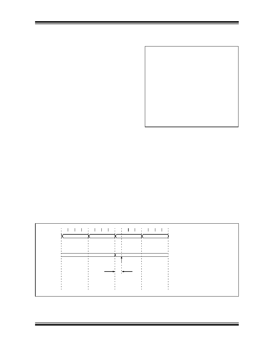
FIGURE 4-10:
SUCCESSIVE I/O OPERATION
;Initial PORT settings: PORTB<7:4> Inputs
;
PORTB<3:0> Outputs
;PORTB<7:6> have external pull-ups and are
;not connected to other circuitry
;
PORT latch
PORT pins
;
----------
---------
BCF PORTB,
7
; 01pp pppp
11pp pppp
BCF PORTB,
6
; 10pp pppp
11pp pppp
BCF STATUS, RP1 ; Select Bank1
BSF STATUS, RP0 ;
BCF TRISB,
7
; 10pp pppp
11pp pppp
BCF TRISB,
6
; 10pp pppp
10pp pppp
;
;Note that the user may have expected the
;pin values to be 00pp ppp. The 2nd BCF
;caused RB7 to be latched as the pin value
;(high).
PC
PC + 1
PC + 2
PC + 3
Q1 Q2 Q3 Q4
Q1
Q2 Q3 Q4 Q1 Q2 Q3 Q4
Q1 Q2 Q3 Q4
Instruction
Fetched
RB7:RB0
MOVWF PORTB
write to
PORTB
NOP
Port pin
sampled here
NOP
MOVF PORTB,W
Instruction
Executed
MOVWF PORTB
write to
PORTB
NOP
MOVF PORTB,W
PC
TPD
Note:
This example shows a write to PORTB
followed by a read from PORTB.
Note that:
data setup time = (0.25TCY - TPD)
where TCY
=
instruction cycle
TPD
=
propagation delay
Therefore, at higher clock frequencies,
a write followed by a read may be
problematic.
相關(guān)PDF資料 |
PDF描述 |
|---|---|
| PIC16C925/PT | 8-BIT, OTPROM, 20 MHz, RISC MICROCONTROLLER, PQFP64 |
| PIC16LC926-I/PT | 8-BIT, OTPROM, 10 MHz, RISC MICROCONTROLLER, PQFP64 |
| PIC16F1518-I/SO | 8-BIT, FLASH, RISC MICROCONTROLLER, PDSO28 |
| PIC16F1518T-E/MV | RISC MICROCONTROLLER, PQCC28 |
| PIC16LF1519-E/MV | 8-BIT, FLASH, RISC MICROCONTROLLER, PQCC40 |
相關(guān)代理商/技術(shù)參數(shù) |
參數(shù)描述 |
|---|---|
| PIC16C925T-I/L | 功能描述:8位微控制器 -MCU 7KB 176 RAM 52 I/O RoHS:否 制造商:Silicon Labs 核心:8051 處理器系列:C8051F39x 數(shù)據(jù)總線(xiàn)寬度:8 bit 最大時(shí)鐘頻率:50 MHz 程序存儲(chǔ)器大小:16 KB 數(shù)據(jù) RAM 大小:1 KB 片上 ADC:Yes 工作電源電壓:1.8 V to 3.6 V 工作溫度范圍:- 40 C to + 105 C 封裝 / 箱體:QFN-20 安裝風(fēng)格:SMD/SMT |
| PIC16C925T-I/PT | 功能描述:8位微控制器 -MCU 7KB 176 RAM 52 I/O RoHS:否 制造商:Silicon Labs 核心:8051 處理器系列:C8051F39x 數(shù)據(jù)總線(xiàn)寬度:8 bit 最大時(shí)鐘頻率:50 MHz 程序存儲(chǔ)器大小:16 KB 數(shù)據(jù) RAM 大小:1 KB 片上 ADC:Yes 工作電源電壓:1.8 V to 3.6 V 工作溫度范圍:- 40 C to + 105 C 封裝 / 箱體:QFN-20 安裝風(fēng)格:SMD/SMT |
| PIC16C926/CL | 功能描述:8位微控制器 -MCU 14KB 336 RAM 52 I/O RoHS:否 制造商:Silicon Labs 核心:8051 處理器系列:C8051F39x 數(shù)據(jù)總線(xiàn)寬度:8 bit 最大時(shí)鐘頻率:50 MHz 程序存儲(chǔ)器大小:16 KB 數(shù)據(jù) RAM 大小:1 KB 片上 ADC:Yes 工作電源電壓:1.8 V to 3.6 V 工作溫度范圍:- 40 C to + 105 C 封裝 / 箱體:QFN-20 安裝風(fēng)格:SMD/SMT |
| PIC16C926-I/L | 功能描述:8位微控制器 -MCU 14KB 336 RAM 52 I/O RoHS:否 制造商:Silicon Labs 核心:8051 處理器系列:C8051F39x 數(shù)據(jù)總線(xiàn)寬度:8 bit 最大時(shí)鐘頻率:50 MHz 程序存儲(chǔ)器大小:16 KB 數(shù)據(jù) RAM 大小:1 KB 片上 ADC:Yes 工作電源電壓:1.8 V to 3.6 V 工作溫度范圍:- 40 C to + 105 C 封裝 / 箱體:QFN-20 安裝風(fēng)格:SMD/SMT |
| PIC16C926-I/L | 制造商:Microchip Technology Inc 功能描述:8BIT CMOS MCU SMD 16C926 PLCC68 |
發(fā)布緊急采購(gòu),3分鐘左右您將得到回復(fù)。