- 您現(xiàn)在的位置:買賣IC網(wǎng) > PDF目錄1961 > PI74SSTU32864ANBE (Pericom)IC 25BIT CONFIG REG BUFF 96LFBGA PDF資料下載
參數(shù)資料
| 型號: | PI74SSTU32864ANBE |
| 廠商: | Pericom |
| 文件頁數(shù): | 1/10頁 |
| 文件大小: | 0K |
| 描述: | IC 25BIT CONFIG REG BUFF 96LFBGA |
| 產(chǎn)品變化通告: | Product Discontinuation Notice 22/Jan/2010 |
| 標準包裝: | 285 |
| 應用: | DDR2 RDIMM |
| 接口: | 差分 |
| 電源電壓: | 1.7 V ~ 1.9 V |
| 封裝/外殼: | 96-LFBGA |
| 供應商設備封裝: | 96-LFBGA(13.5x5.5) |
| 包裝: | 托盤 |
| 安裝類型: | 表面貼裝 |
1
PS8743
08/02/04
Features
PI74SSTU32864A is designed for low-voltage operation,
VDD = 1.8V
Supports Low Power Standby Operation
Enhanced Signal Integrity for 1 and 2 Rank Modules
All Inputs are SSTL_18 Compatible, except RST, C0, C1,
which are LVCMOS.
Output drivers are optimized to drive DDR2 DIMM loads
Designed for DDR2 Memory
Packaging (Pb-free & Green available):
-96 Ball LFBGA (NB)
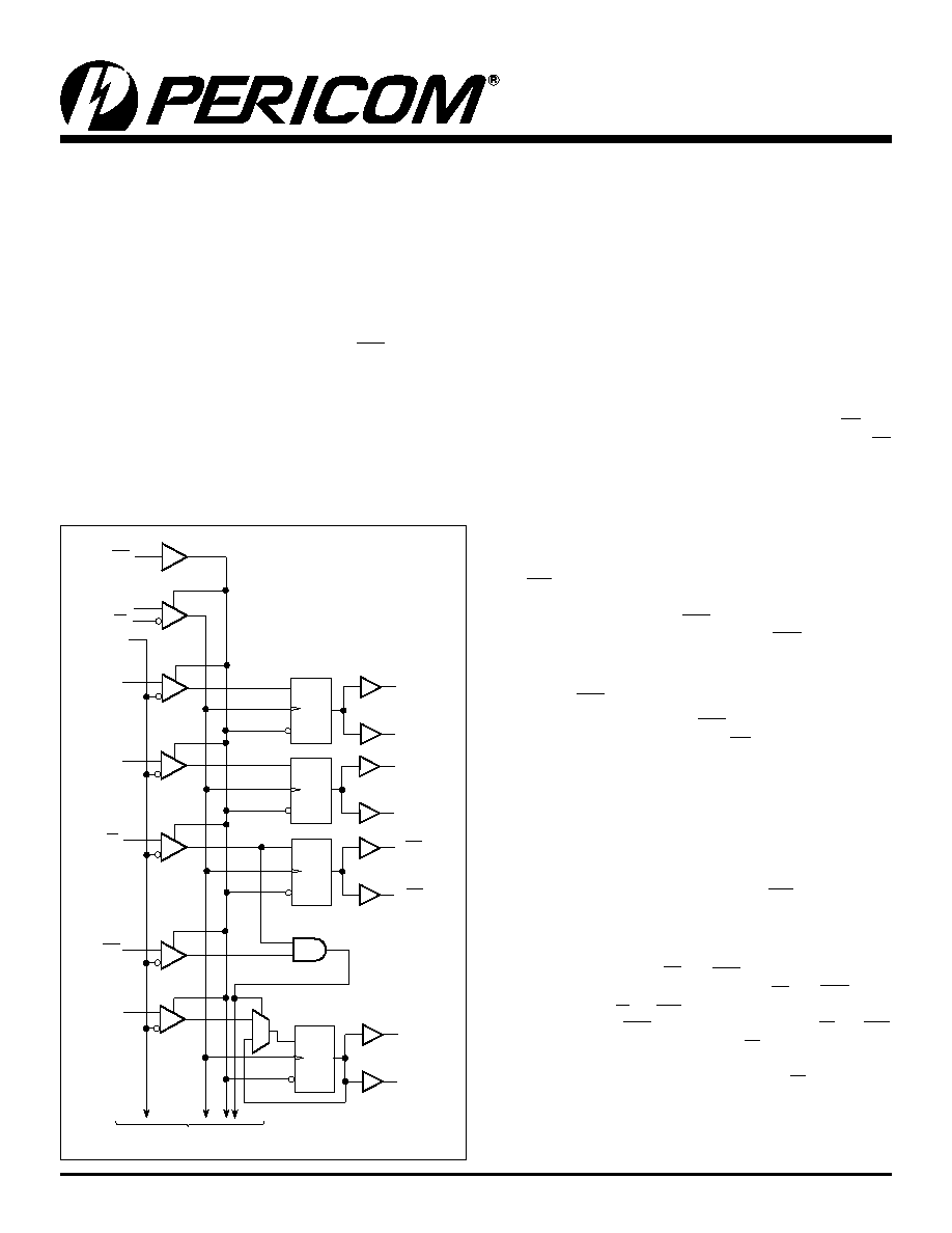
Block Diagram 1:2 Mode (Positive Logic)
PI74SSTU32864A
25-Bit 1:1 or 14-Bit 1:2 Configurable
Registered Buffer
TO OTHER CHANNELS
CK
RST
1D
C1
R
QCKEA
QCKEB*
QODTA
1D
C1
R
Q1A
Q1B*
QCSB*
QCSA
1D
C1
R
1D
C1
R
QODTB*
VREF
DCKE
DODT
DCS
CSR
D1
Note: Disabled in 1:1 configuration
0
1
Description
Pericom Semiconductor’s PI74SSTU32864A logic circuit is
produced using advanced CMOS technology. This 25-Bit 1:1 or
14-Bit 1:2 configurable registered buffer is designed for 1.7V to
1.9V VDD operation.
All clock and data inputs are compatible with the JEDEC standard
for SSTL_18. The control inputs are LVCMOS. All outputs are
1.8V LVCMOS drivers that have been optimized to drive the
DDR2 DIMM load.
The SSTU32864A operates from a differential clock (CK and
CK). Data is registered at the crossing of CK going high, and CK
going low.
The C0 input controls the pinout configuration of the 1:2 pinout
from A configuration (when LOW) to B configuration (when
HIGH). The C1 input controls the pinout configuration for 25-Bit
1:1 (when LOW) to 14-Bit 1:2 (when HIGH).
The device supports low-power standby operation. When the reset
input (RST) is low, the differential input receivers are disabled and
undriven (floating) data, clock and reference voltage (VREF) inputs
are allowed. In addition , when RST is low, all registers are reset,
and all outputs are forced low. The LVCMOS RST and Cn inputs
must always be held at a valid logic high or low level.
To ensure defined outputs from the register before a stable clock has
been supplied, RST must be held in the low state during power up.
IntheDDR-IIRDIMMapplication,RSTisspecifiedtobecompletely
asynchronous with respect to CK and CK. Therefore, no timing
relationship can be guaranteed between the two. When entering
reset, the register will be cleared and the outputs will be driven
low quickly, relative to the time to disable the differential input
receivers. However, when coming out of reset, the register will
become active quickly, relative to the time to enable the differential
input receivers.
As long as the data inputs are low, and the clock is stable during
the time from the low-to-high transition of RST until the input
receivers are fully enabled, the design of the SSTU32864A must
ensure that the outputs remain low, thus ensuring no glitches on
the output.
The device monitors both DCS and CSR inputs and will gate the
Qn outputs from changing states when both DCS and CSR inputs
are high. If either DCS or CSR input is low, the Qn outputs will
functionnormally.TheRSTinputhaspriorityovertheDCSandCSR
control will force the outputs low. If the DCS control functionality
is not desired, then the CSR input can be hardwired to ground,
in which case, the set-up time requirement for DCS would be the
same as for the other D data inputs.
相關PDF資料 |
PDF描述 |
|---|---|
| PI7AT04CEX | IC TRANSMISSION LINE CLMP SC70-6 |
| PI7C7300ANAE | IC PCI-PCI BRIDGE 3PORT 272-BGA |
| PI7C7300DNAE | IC PCI-PCI BRIDGE 3PORT 272-BGA |
| PI7C8140AMAE | IC PCI-PCI BRIDGE 2PORT 128-QFP |
| PI7C8150ANDE | IC PCI-PCI BRIDGE 2PORT 256-PBGA |
相關代理商/技術參數(shù) |
參數(shù)描述 |
|---|---|
| PI74SSTU32864ANBEX | 功能描述:寄存器 25B 1:1 or 14B 1:2 RoHS:否 制造商:NXP Semiconductors 邏輯類型:CMOS 邏輯系列:HC 電路數(shù)量:1 最大時鐘頻率:36 MHz 傳播延遲時間: 高電平輸出電流:- 7.8 mA 低電平輸出電流:7.8 mA 電源電壓-最大:6 V 最大工作溫度:+ 125 C 封裝 / 箱體:SOT-38 封裝:Tube |
| PI74SSTU32864NBE | 功能描述:寄存器 25B 1:1 or 14B 1:2 RoHS:否 制造商:NXP Semiconductors 邏輯類型:CMOS 邏輯系列:HC 電路數(shù)量:1 最大時鐘頻率:36 MHz 傳播延遲時間: 高電平輸出電流:- 7.8 mA 低電平輸出電流:7.8 mA 電源電壓-最大:6 V 最大工作溫度:+ 125 C 封裝 / 箱體:SOT-38 封裝:Tube |
| PI74SSTU32864NBEX | 功能描述:寄存器 25B 1:1 or 14B 1:2 RoHS:否 制造商:NXP Semiconductors 邏輯類型:CMOS 邏輯系列:HC 電路數(shù)量:1 最大時鐘頻率:36 MHz 傳播延遲時間: 高電平輸出電流:- 7.8 mA 低電平輸出電流:7.8 mA 電源電壓-最大:6 V 最大工作溫度:+ 125 C 封裝 / 箱體:SOT-38 封裝:Tube |
| PI74SSTU32866NBE | 功能描述:寄存器 25B 1:1 or 14B 1:2 RoHS:否 制造商:NXP Semiconductors 邏輯類型:CMOS 邏輯系列:HC 電路數(shù)量:1 最大時鐘頻率:36 MHz 傳播延遲時間: 高電平輸出電流:- 7.8 mA 低電平輸出電流:7.8 mA 電源電壓-最大:6 V 最大工作溫度:+ 125 C 封裝 / 箱體:SOT-38 封裝:Tube |
| PI74SSTU32866NBEX | 功能描述:寄存器 25B 1:1 or 14B 1:2 RoHS:否 制造商:NXP Semiconductors 邏輯類型:CMOS 邏輯系列:HC 電路數(shù)量:1 最大時鐘頻率:36 MHz 傳播延遲時間: 高電平輸出電流:- 7.8 mA 低電平輸出電流:7.8 mA 電源電壓-最大:6 V 最大工作溫度:+ 125 C 封裝 / 箱體:SOT-38 封裝:Tube |
發(fā)布緊急采購,3分鐘左右您將得到回復。