- 您現(xiàn)在的位置:買賣IC網(wǎng) > PDF目錄367938 > PHD34NQ10T (NXP SEMICONDUCTORS) N-channel TrenchMOS transistor(N溝道TrenchMOS 晶體管邏輯電平場(chǎng)效應(yīng)管) PDF資料下載
參數(shù)資料
| 型號(hào): | PHD34NQ10T |
| 廠商: | NXP SEMICONDUCTORS |
| 元件分類: | JFETs |
| 英文描述: | N-channel TrenchMOS transistor(N溝道TrenchMOS 晶體管邏輯電平場(chǎng)效應(yīng)管) |
| 中文描述: | 35 A, 100 V, 0.04 ohm, N-CHANNEL, Si, POWER, MOSFET, TO-252 |
| 封裝: | PLASTIC, SC-63, DPAK-3 |
| 文件頁數(shù): | 2/12頁 |
| 文件大?。?/td> | 115K |
| 代理商: | PHD34NQ10T |
Philips Semiconductors
Product specification
N-channel TrenchMOS
transistor
PHP34NQ10T, PHB34NQ10T
PHD34NQ10T
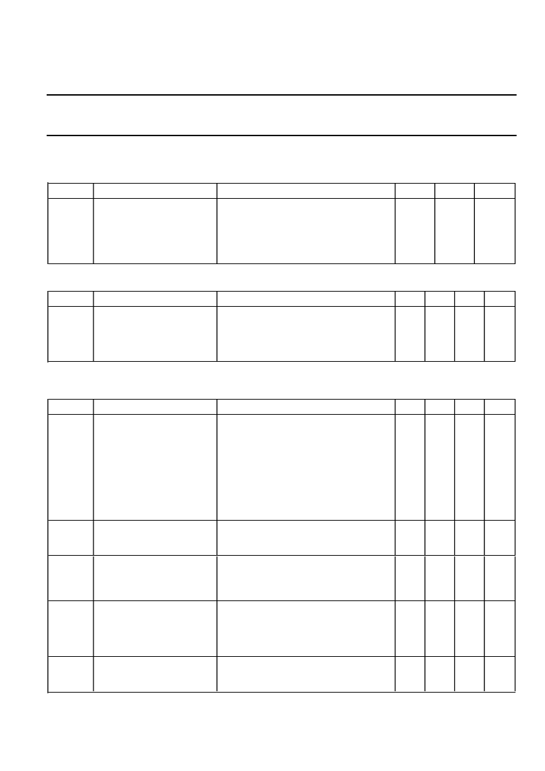
AVALANCHE ENERGY LIMITING VALUES
Limiting values in accordance with the Absolute Maximum System (IEC 134)
SYMBOL PARAMETER
E
AS
Non-repetitive avalanche
energy
CONDITIONS
Unclamped inductive load, I
= 26 A;
t
p
= 100
μ
s; T
j
prior to avalanche = 25C;
V
≤
25 V; R
GS
= 50
; V
GS
= 10 V; refer
to fig:15
MIN.
-
MAX.
170
UNIT
mJ
I
AS
Peak non-repetitive
avalanche current
-
35
A
THERMAL RESISTANCES
SYMBOL PARAMETER
R
th j-mb
Thermal resistance junction
to mounting base
R
th j-a
Thermal resistance junction
to ambient
CONDITIONS
MIN.
-
TYP. MAX. UNIT
-
1.1
K/W
SOT78 package, in free air
SOT404 & SOT428 packages, pcb
mounted, minimum footprint
-
-
60
50
-
-
K/W
K/W
ELECTRICAL CHARACTERISTICS
T
j
= 25C unless otherwise specified
SYMBOL PARAMETER
V
(BR)DSS
Drain-source breakdown
voltage
V
GS(TO)
Gate threshold voltage
CONDITIONS
V
GS
= 0 V; I
D
= 0.25 mA;
MIN.
100
89
2
1
-
-
-
-
-
-
-
-
-
TYP. MAX. UNIT
-
-
-
-
3
4
-
-
6
35
40
-
108
10
100
0.05
10
-
500
40
-
7
-
18
-
V
V
V
V
V
T
j
= -55C
V
DS
= V
GS
; I
D
= 1 mA
T
j
= 175C
T
j
= -55C
R
DS(ON)
Drain-source on-state
resistance
Gate source leakage current V
GS
=
±
10 V; V
DS
= 0 V
Zero gate voltage drain
current
Total gate charge
Gate-source charge
Gate-drain (Miller) charge
V
GS
= 10 V; I
D
= 17 A
m
m
nA
μ
A
μ
A
nC
nC
nC
T
j
= 175C
I
GSS
I
DSS
V
DS
= 100 V; V
GS
= 0 V
T
j
= 175C
Q
g(tot)
Q
gs
Q
gd
t
d on
t
r
t
d off
t
f
L
d
L
d
I
D
= 34 A; V
DD
= 80 V; V
GS
= 10 V
Turn-on delay time
Turn-on rise time
Turn-off delay time
Turn-off fall time
Internal drain inductance
Internal drain inductance
V
DD
= 50 V; R
D
= 1.5
;
V
= 10 V; R
G
= 5.6
Resistive load
-
-
-
-
-
-
12
55
48
38
3.5
4.5
-
-
-
-
-
-
ns
ns
ns
ns
nH
nH
Measured tab to centre of die
Measured from drain lead to centre of die
(SOT78 package only)
Measured from source lead to source
bond pad
V
GS
= 0 V; V
DS
= 25 V; f = 1 MHz
L
s
Internal source inductance
-
7.5
-
nH
C
iss
C
oss
C
rss
Input capacitance
Output capacitance
Feedback capacitance
-
-
-
1704
227
140
-
-
-
pF
pF
pF
August 1999
2
Rev 1.000
相關(guān)PDF資料 |
PDF描述 |
|---|---|
| PHP34NQ10T | N-channel TrenchMOS transistor(N溝道TrenchMOS 晶體管邏輯電平場(chǎng)效應(yīng)管) |
| PHB36N06E | PowerMOS transistor |
| PHB37N06T | TrenchMOS transistor Standard level FET |
| PHB3N50E | PowerMOS transistors Avalanche energy rated |
| PHP3N50E | PowerMOS transistors Avalanche energy rated |
相關(guān)代理商/技術(shù)參數(shù) |
參數(shù)描述 |
|---|---|
| PHD34NQ10T /T3 | 功能描述:兩極晶體管 - BJT TAPE13 MOSFET RoHS:否 制造商:STMicroelectronics 配置: 晶體管極性:PNP 集電極—基極電壓 VCBO: 集電極—發(fā)射極最大電壓 VCEO:- 40 V 發(fā)射極 - 基極電壓 VEBO:- 6 V 集電極—射極飽和電壓: 最大直流電集電極電流: 增益帶寬產(chǎn)品fT: 直流集電極/Base Gain hfe Min:100 A 最大工作溫度: 安裝風(fēng)格:SMD/SMT 封裝 / 箱體:PowerFLAT 2 x 2 |
| PHD34NQ10T,118 | 功能描述:MOSFET TAPE13 MOSFET RoHS:否 制造商:STMicroelectronics 晶體管極性:N-Channel 汲極/源極擊穿電壓:650 V 閘/源擊穿電壓:25 V 漏極連續(xù)電流:130 A 電阻汲極/源極 RDS(導(dǎo)通):0.014 Ohms 配置:Single 最大工作溫度: 安裝風(fēng)格:Through Hole 封裝 / 箱體:Max247 封裝:Tube |
| PHD36070G | 制造商:Schneider Electric 功能描述:BUSWAY CB PLUG-IN, 70A, H FRAME |
| PHD36N03LT | 制造商:PHILIPS 制造商全稱:NXP Semiconductors 功能描述:N-channel TrenchMOS logic level FET |
| PHD36N03LT /T3 | 功能描述:兩極晶體管 - BJT TAPE13 MOSFET RoHS:否 制造商:STMicroelectronics 配置: 晶體管極性:PNP 集電極—基極電壓 VCBO: 集電極—發(fā)射極最大電壓 VCEO:- 40 V 發(fā)射極 - 基極電壓 VEBO:- 6 V 集電極—射極飽和電壓: 最大直流電集電極電流: 增益帶寬產(chǎn)品fT: 直流集電極/Base Gain hfe Min:100 A 最大工作溫度: 安裝風(fēng)格:SMD/SMT 封裝 / 箱體:PowerFLAT 2 x 2 |
發(fā)布緊急采購,3分鐘左右您將得到回復(fù)。