- 您現(xiàn)在的位置:買賣IC網(wǎng) > PDF目錄382384 > PCO24 PC(ISA)BUS I/O CARD PDF資料下載
參數(shù)資料
| 型號: | PCO24 |
| 英文描述: | PC(ISA)BUS I/O CARD |
| 中文描述: | 電腦(ISA)總線的I / O卡 |
| 文件頁數(shù): | 5/13頁 |
| 文件大小: | 192K |
| 代理商: | PCO24 |

C ONTR OL S YS TE MS
J224 PCO24
2192-10479-000-000
Page 4
Operation
Reading or Writing to the Board
Control of the PCO24 is achieved by writing to a pointer register and then accessing a data
register to read or write the required I/O register. The pointer register need only be written with
a new value if a different register is to be accessed. The board occupies only two bytes of
PCbus I/O space. Each time the board is accessed the red LED will flash momentarily.
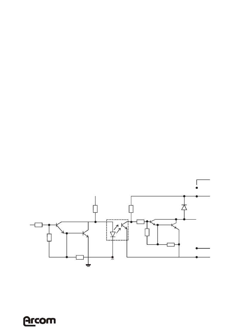
Opto-isolated Outputs
There are three groups each of 8 bits connected via opto-isolators to the D connector. They
are considered as a group as all eight bits are written to at the same time.
Using group 0 bit 0 as an example.
If LK1 is in position A it is necessary to enable the outputs. This is done by writing 90h to the
base address, which sets the pointer to the output enable register. Now write 01 to base
address +1. The output of IC30 will enable all outputs. If LK1 is in position B the outputs will
always be enabled. Now you can write to the outputs. Firstly set the pointer register to the
group i.e. write 00 to base address, this points to group 0 register and then write the value to
base address +1. You can also read back that value by reading base address +1.
Writing a ‘1’ to an output switches the output low; i.e. it is sinking current. During system
initialisation it is recommended that the values to be output are written to the output registers
prior to enabling the output channels.
Data
2k7
7k
3k
470k
+5
15k
2k7
COMMON +
GROUP 0+
COMMON OV
GROUP 0 OV
LK10
LK11
相關(guān)PDF資料 |
PDF描述 |
|---|---|
| PCT-1611 | Transformer |
| PCT-1616 | Transformer |
| PCT-1617 | MODEM TRANSFORMER |
| PCT-1618 | MODEM TRANSFORMER |
| PCT-1612 | MODEM TRANSFORMER |
相關(guān)代理商/技術(shù)參數(shù) |
參數(shù)描述 |
|---|---|
| PCO-7120 | 制造商:IXYS Corporation 功能描述:Laser Driver 1-CH |
| PCOF12864B-BCFBD | 制造商:P-TEC 制造商全稱:P-tec Corporation 功能描述:240 Column X 64 Row |
| PCOF12864B-BCFGD | 制造商:P-TEC 制造商全稱:P-tec Corporation 功能描述:240 Column X 64 Row |
| PCOF12864B-BCFOD | 制造商:P-TEC 制造商全稱:P-tec Corporation 功能描述:240 Column X 64 Row |
| PCOF12864B-BCFSD | 制造商:P-TEC 制造商全稱:P-tec Corporation 功能描述:240 Column X 64 Row |
發(fā)布緊急采購,3分鐘左右您將得到回復。