- 您現(xiàn)在的位置:買賣IC網(wǎng) > PDF目錄382379 > PCA9545PW (NXP SEMICONDUCTORS) 4-channel I2C switch with interrupt logic and reset PDF資料下載
參數(shù)資料
| 型號: | PCA9545PW |
| 廠商: | NXP SEMICONDUCTORS |
| 元件分類: | 通用總線功能 |
| 英文描述: | 4-channel I2C switch with interrupt logic and reset |
| 中文描述: | 9545 SERIES, 4 LINE TO 1 LINE MULTIPLEXER, TRUE OUTPUT, PDSO20 |
| 封裝: | 4.40 MM, PLASTIC, MO-153, SOT-360-1, TSSOP-20 |
| 文件頁數(shù): | 9/14頁 |
| 文件大小: | 118K |
| 代理商: | PCA9545PW |
Philips Semiconductors
Product data
PCA9545
4-channel I
2
C switch with interrupt logic and reset
2002 Mar 28
9
853-2302 27311
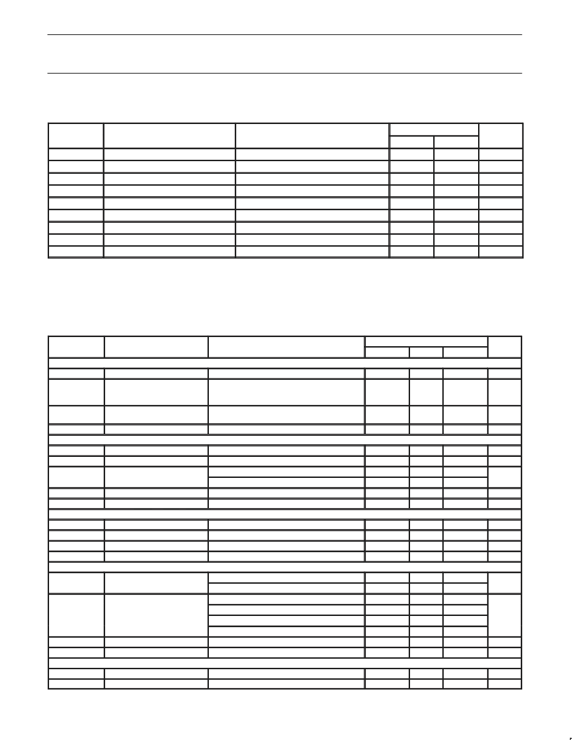
ABSOLUTE MAXIMUM RATINGS
1, 2
In accordance with the Absolute Maximum Rating System (IEC 134).Voltages are referenced to GND (ground = 0 V).
SYMBOL
PARAMETER
CONDITIONS
RATING
UNIT
MIN
–0.5
–0.5
—
—
—
—
—
–60
–40
MAX
+7.0
+7.0
±
20
±
25
±
100
±
100
400
+150
+85
V
DD
V
I
I
I
I
O
I
DD
I
SS
P
tot
T
stg
T
amb
DC supply voltage
DC input voltage
DC input current
DC output current
DC Supply current
DC Supply current
total power dissipation
Storage temperature range
Operating ambient temperature
V
V
mA
mA
mA
mA
mW
°
C
°
C
NOTES:
1. Stresses beyond those listed may cause permanent damage to the device. These are stress ratings only and functional operation of the
device at these or any other conditions beyond those indicated under “recommended operating conditions” is not implied. Exposure to
absolute-maximum-rated conditions for extended periods may affect device reliability.
2. The performance capability of a high-performance integrated circuit in conjunction with its thermal environment can create junction
temperatures which are detrimental to reliability. The maximum junction temperature of this integrated circuit should not exceed 150
°
C.
DC CHARACTERISTICS
V
DD
= 2.3 to 3.6 V; V
SS
= 0 V; T
amb
= –40 to +85
°
C; unless otherwise specified. (See page 11 for V
DD
= 3.6 to 5.5 V.)
SYMBOL
PARAMETER
TEST CONDITIONS
LIMITS
TYP
UNIT
MIN
MAX
Supply
V
DD
Supply voltage
2.3
—
3.6
V
I
DD
Supply current
Operating mode; V
DD
= 3.6 V;
no load; V
= V
or V
SS
;
f
SCL
= 100 kHz
Standby mode; V
DD
= 3.6 V;
no load; V
I
= V
DD
or V
SS
no load; V
I
= V
DD
or V
SS
—
30
100
μ
A
I
stb
Standby current
—
20
100
μ
A
V
POR
Power-on reset voltage
—
1.6
2.1
V
Input SCL; input/output SDA
V
IL
V
IH
LOW level input voltage
HIGH level input voltage
–0.5
0.7 V
DD
3
6
–1
—
—
—
—
—
—
12
0.3 V
DD
6
—
—
+1
13
V
V
I
OL
LOW level output current
LOW level out ut current
V
OL
= 0.4 V
V
OL
= 0.6 V
V
I
= V
DD
or V
SS
V
I
= V
SS
mA
I
L
C
i
Leakage current
Input capacitance
μ
A
pF
Select inputs A0 to A1 / INT0 to INT3 / RESET
V
IL
LOW level input voltage
V
IH
HIGH level input voltage
I
LI
Input leakage current
C
i
Input capacitance
Pass Gate
–0.5
0.7 V
DD
–1
—
—
—
—
1.6
+0.3 V
DD
V
DD
+ 0.5
+1
3
V
V
μ
A
pF
pin at V
DD
or V
SS
V
I
= V
SS
R
ON
Switch resistance
V
DD
= 3.0 to 3.6 V, V
O
= 0.4 V, I
O
= 15 mA
V
DD
= 2.3 to 2.7 V, V
O
= 0.4 V, I
O
= 10 mA
V
swin
= V
DD
= 3.3 V; I
swout
= –100
μ
A
V
swin
= V
DD
= 3.0 to 3.6 V; I
swout
= –100
μ
A
V
swin
= V
DD
= 2.5 V; I
swout
= –100
μ
A
V
swin
= V
DD
= 2.3 to 2.7 V; I
= –100
μ
A
V
I
= V
DD
or V
SS
V
I
= V
SS
5
7
—
1.6
—
1.1
–1
—
20
26
2.2
—
1.5
—
—
3
30
55
—
2.8
—
2.0
+1
5
V
Pass
Switch output voltage
Switch out ut voltage
V
I
L
C
io
Leakage current
Input/output capacitance
μ
A
pF
INT Output
I
OL
I
OH
LOW level output current
HIGH level output current
V
OL
= 0.4 V
3
—
—
—
—
mA
μ
A
+100
相關(guān)PDF資料 |
PDF描述 |
|---|---|
| PCA9548A | 8-channel I2C switch with reset |
| PCA9548 | 8-channel I2C switch with reset |
| PCA9548D | 8-channel I2C switch with reset |
| PCA9548PW | 8-channel I2C switch with reset |
| PCA9550 | 2-bit I2C LED driver with programmable blink rates |
相關(guān)代理商/技術(shù)參數(shù) |
參數(shù)描述 |
|---|---|
| PCA9546 | 制造商:PHILIPS 制造商全稱:NXP Semiconductors 功能描述:4-channel I2C switch with reset |
| PCA9546A | 制造商:TI 制造商全稱:Texas Instruments 功能描述:4-CHANNEL I2C AND SMBus SWITCH WITH RESET FUNCTION |
| PCA9546A_1 | 制造商:TI 制造商全稱:Texas Instruments 功能描述:4-CHANNEL I2C AND SMBus SWITCH WITH RESET FUNCTION |
| PCA9546A_2 | 制造商:TI 制造商全稱:Texas Instruments 功能描述:4-CHANNEL I2C AND SMBus SWITCH WITH RESET FUNCTION |
| PCA9546A_3 | 制造商:TI 制造商全稱:Texas Instruments 功能描述:4-CHANNEL I2C AND SMBus SWITCH WITH RESET FUNCTION |
發(fā)布緊急采購,3分鐘左右您將得到回復(fù)。