- 您現(xiàn)在的位置:買賣IC網(wǎng) > PDF目錄384824 > P4C149-15LSM (Pyramid Semiconductor Corporation) ULTRA HIGH SPEED 1K x 4 STATIC CMOS RAMS PDF資料下載
參數(shù)資料
| 型號: | P4C149-15LSM |
| 廠商: | Pyramid Semiconductor Corporation |
| 英文描述: | ULTRA HIGH SPEED 1K x 4 STATIC CMOS RAMS |
| 中文描述: | 超高速每1000 × 4靜態(tài)CMOS五羊 |
| 文件頁數(shù): | 3/10頁 |
| 文件大小: | 289K |
| 代理商: | P4C149-15LSM |
P4C148/P4C149
Page 3 of 10
Document #
SRAM104
REV B
Notes:
1. Stresses greater than those listed under MAXIMUM RATINGS may
cause permanent damage to the device. This is a stress rating only
and functional operation of the device at these or any other
conditions above those indicated in the operational sections of this
specification is not implied. Exposure to MAXIMUM rating condi-
tions for extended periods may affect reliability.
2. Extended temperature operation guaranteed with 400 linear feet
per minute of air flow.
3. Transient inputs with V
IL
and I
IL
not more negative than –3.0V and
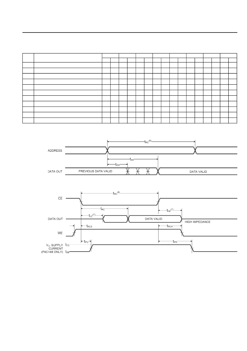
TIMING WAVEFORM OF READ CYCLE NO. 2
(6)
TIMING WAVEFORM OF READ CYCLE
AC CHARACTERISTICS—READ CYCLE
(V
CC
= 5V ± 10%, All Temperature Ranges)
(2)
–100mA, respectively, are permissible for pulse widths up to 20 ns.
4. This parameter is sampled and not 100% tested.
5.
CE
is LOW and
WE
is HIGH for READ cycle.
6.
WE
is HIGH, and address must be valid prior to or coincident with
CE
transition LOW.
7. Transition is measured ±200mV from steady state voltage prior to
change with specified loading in Figure 1. This parameter is
sampled and not 100% tested.
8. Read Cycle Time is measured from the last valid address to the first
transitioning address.
Min Max Min Max Min Max Min Max Min Max Min Max Min Max Min Max
10
12
15
20
t
RC
t
AA
t
AC
t
AC
t
OH
t
LZ
t
HZ
t
RCS
t
RCH
t
PU
t
PD
Read Cycle Time
25
35
45
55
Address Access Time
Chip Enable Access Time (P4C148)
10
10
12
12
15
15
20
20
25
25
35
35
45
45
55
55
Chip Enable Access Time (P4C149)
8
10
12
14
15
20
20
25
Output Hold from Address Change
Chip Enable to Output in Low Z (P4C149)
3
2
3
2
3
2
3
2
3
2
3
2
3
2
3
2
Chip Disable to Output in High Z (P4C149)
4
5
6
8
10
14
18
20
Read Command Setup Time
Read Command Hold Time
0
0
0
0
0
0
0
0
0
0
0
0
0
0
0
0
Chip Enable to Power Up Time (P4C148)
0
0
0
0
0
0
0
0
Chip Disable to Power Down Time (P4C148)
10
12
15
20
25
35
45
55
-45
-55
-15
-20
-25
-35
Sym
Parameter
-10
-12
相關(guān)PDF資料 |
PDF描述 |
|---|---|
| P4C149-15LSMB | ULTRA HIGH SPEED 1K x 4 STATIC CMOS RAMS |
| P4C149-15PM | ULTRA HIGH SPEED 1K x 4 STATIC CMOS RAMS |
| P4C149-15PMB | ULTRA HIGH SPEED 1K x 4 STATIC CMOS RAMS |
| P4C149-20CC | ULTRA HIGH SPEED 1K x 4 STATIC CMOS RAMS |
| P4C149-20CM | ULTRA HIGH SPEED 1K x 4 STATIC CMOS RAMS |
相關(guān)代理商/技術(shù)參數(shù) |
參數(shù)描述 |
|---|---|
| P4C164-20L32MB | 制造商:Micross Components 功能描述:SRAM ASYNC SGL 5V 64KBIT 8KX8 20NS 32PIN LCC - Bulk |
| P4C164-55L32MB | 制造商:Micross Components 功能描述:SRAM ASYNC SGL 5V 64KBIT 8KX8 55NS 32PIN LCC - Bulk |
| P4C164-70L32MB | 制造商:Micross Components, Inc. 功能描述:SRAM ASYNC SGL 5V 64KBIT 8KX8 70NS 32PIN LCC - Bulk |
| P4C164L-45L32MB | 制造商:Micross Components, Inc. 功能描述:8KX8 SRAM - Bulk |
| P4C168125PI | 制造商:PERFORMANC 功能描述:* |
發(fā)布緊急采購,3分鐘左右您將得到回復(fù)。