- 您現(xiàn)在的位置:買賣IC網(wǎng) > PDF目錄384809 > P4C1048L-45TC (PYRAMID SEMICONDUCTOR CORP) LOW POWER 512K x 8 CMOS STATIC RAM PDF資料下載
參數(shù)資料
| 型號: | P4C1048L-45TC |
| 廠商: | PYRAMID SEMICONDUCTOR CORP |
| 元件分類: | DRAM |
| 英文描述: | LOW POWER 512K x 8 CMOS STATIC RAM |
| 中文描述: | 512K X 8 STANDARD SRAM, 45 ns, PDSO32 |
| 封裝: | PLASTIC, TSOP2-32 |
| 文件頁數(shù): | 7/12頁 |
| 文件大?。?/td> | 168K |
| 代理商: | P4C1048L-45TC |
P4C1048L
Page 7 of 12
Document #
SRAM129
REV D
Write
Active
Active
Read
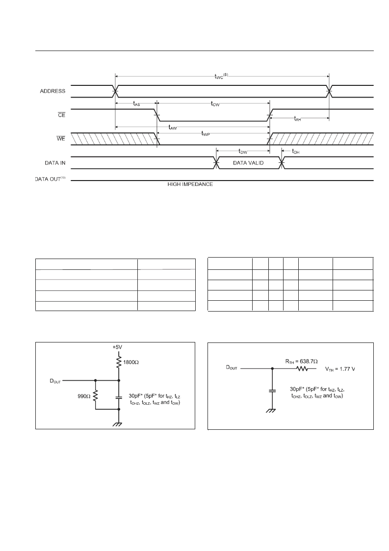
TIMING WAVEFORM OF WRITE CYCLE NO.2 (
CE
CONTROLLED)
(6)
* including scope and test fixture.
Note:
Because of the high speed of the P4C1048L, care must be taken when
testing this device; an inadequate setup can cause a normal functioning
part to be rejected as faulty. Long high-inductance leads that cause
supply bounce must be avoided by bringing the V
and ground planes
directly up to the contactor fingers. A 0.01 μF high frequency capacitor
is also required between V
CC
and ground.
To avoid signal reflections, proper termination must be used; for example,
a 50
test environment should be terminated into a 50
load with 1.77V
(Thevenin Voltage) at the comparator input, and a 589
resistor must be
used in series with D
OUT
to match 639
(Thevenin Resistance).
AC TEST CONDITIONS
TRUTH TABLE
Input Pulse Levels
Input Rise and Fall Times
Input Timing Reference Level
Output Timing Reference Level
Output Load
GND to 3.0V
3ns
1.5V
1.5V
See Fig. 1 and 2
Mode
Standby
D
OUT
Disabled
Standby
Active
Power
I/O
WE
X
H
H
L
OE
X
H
CE
H
L
L
L
High Z
D
OUT
D
IN
L
X
High Z
Figure 1. Output Load
Figure 2. Thevenin Equivalent
發(fā)布緊急采購,3分鐘左右您將得到回復(fù)。