- 您現(xiàn)在的位置:買賣IC網(wǎng) > PDF目錄367630 > P2600ECRP2 MCU CMOS 44 LD 40MHZ 8K OTP, -40C to +85C, 44-PLCC, T/R PDF資料下載
參數(shù)資料
| 型號: | P2600ECRP2 |
| 英文描述: | MCU CMOS 44 LD 40MHZ 8K OTP, -40C to +85C, 44-PLCC, T/R |
| 中文描述: | SIDAC的| 300V五(公報)最大| 800mA的我(縣)|對92VAR |
| 文件頁數(shù): | 130/161頁 |
| 文件大小: | 986K |
| 代理商: | P2600ECRP2 |
第1頁第2頁第3頁第4頁第5頁第6頁第7頁第8頁第9頁第10頁第11頁第12頁第13頁第14頁第15頁第16頁第17頁第18頁第19頁第20頁第21頁第22頁第23頁第24頁第25頁第26頁第27頁第28頁第29頁第30頁第31頁第32頁第33頁第34頁第35頁第36頁第37頁第38頁第39頁第40頁第41頁第42頁第43頁第44頁第45頁第46頁第47頁第48頁第49頁第50頁第51頁第52頁第53頁第54頁第55頁第56頁第57頁第58頁第59頁第60頁第61頁第62頁第63頁第64頁第65頁第66頁第67頁第68頁第69頁第70頁第71頁第72頁第73頁第74頁第75頁第76頁第77頁第78頁第79頁第80頁第81頁第82頁第83頁第84頁第85頁第86頁第87頁第88頁第89頁第90頁第91頁第92頁第93頁第94頁第95頁第96頁第97頁第98頁第99頁第100頁第101頁第102頁第103頁第104頁第105頁第106頁第107頁第108頁第109頁第110頁第111頁第112頁第113頁第114頁第115頁第116頁第117頁第118頁第119頁第120頁第121頁第122頁第123頁第124頁第125頁第126頁第127頁第128頁第129頁當前第130頁第131頁第132頁第133頁第134頁第135頁第136頁第137頁第138頁第139頁第140頁第141頁第142頁第143頁第144頁第145頁第146頁第147頁第148頁第149頁第150頁第151頁第152頁第153頁第154頁第155頁第156頁第157頁第158頁第159頁第160頁第161頁
PCB Layout
SIDACtor
Data Book
5 - 14
Teccor Electronics
(972) 580-7777
The minimum width and thickness of conductors on a PCB is determined primarily by
the current-carrying capacity required. This current carrying capacity is limited by the
allowable temperature rise of the etched copper conductor. An adjacent ground or
power layer can significantly reduce this temperature rise. A single ground plane can
generally raise the allowed current by 50 percent. An easy approximation can be
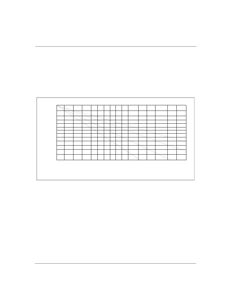
generated by starting with Figure 5-4 to calculate the conductor cross sectional area
required. Once this has been done, Figure 5-5 converts the cross sectional area to the
required conductor width dependent on the copper foil thickness of the trace.
Figure 5-5 Conductor Width vs. Area
Trace Separation
Because Tip and Ring traces are subjected to transient conditions, they should be
routed towards the edge of the PCB away from sensitive areas, and should maintain a
minimum separation of 2.5mm between themselves and other traces. A good rule of
thumb for separation of non-coated top layer traces is to maintain spacing equal to
.010mm per volt.
Grounding
Although often overlooked, grounding is a very important design consideration when
laying out a protection interface circuit. To optimize its effectiveness, several things
should be considered.
The first is that a large copper plane should be provided using a grid pattern for the
ground reference point.
Next, it should be decided if a single point or a multi point grounding scheme is to be
used. A single-point (also called centralized) grounding scheme is used for circuit
dimensions smaller than one-tenth of a wavelength (
λ
= 300,000/F
kHz
) and a multi
point (also called distributed) grounding scheme is used for circuit trace lengths
0
.350
.300
.250
.030
.050
.070
.100
.150
.200
.010
.020
.005
.001
0
1
10
20
100 150
300
400
500
600
700
Conductor Cross-Section Area (sq mils)
5
30 50 70
200
250
C
0
"
7
0
0
0
2
t
o
2
"
4
1
0
0
2
t
o
1
(2oz/ft2 .0028"
(3oz/ft2) .0042"
相關(guān)PDF資料 |
PDF描述 |
|---|---|
| P2600SARP | MCU CMOS 44 LD LOW PWR, -40C to +85C, 44-TQFP, TRAY |
| P2600SBRP | MCU CMOS 40 LD 40MHZ 16K OTP, -40C to +125C, 40-PDIP, TUBE |
| P2600SCRP | SIDAC|300V V(BO) MAX|800MA I(S)|DO-214AA |
| P3000AA61RP | MCU CMOS 44LD LOW PWR, -40C to +85C, 44-QFN, T/R |
| P3002AA | SIDAC|180V V(BO) MAX|800MA I(S)|TO-220VAR |
相關(guān)代理商/技術(shù)參數(shù) |
參數(shù)描述 |
|---|---|
| P2600G_LRP | 制造商:LITTELFUSE 制造商全稱:Littelfuse 功能描述:Teccor㈢ brand Protection Thyristors |
| P2600GALRP | 功能描述:硅對稱二端開關(guān)元件 220V 50A DO15 SIDACtor Bi RoHS:否 制造商:Bourns 轉(zhuǎn)折電流 VBO:40 V 最大轉(zhuǎn)折電流 IBO:800 mA 不重復(fù)通態(tài)電流: 額定重復(fù)關(guān)閉狀態(tài)電壓 VDRM:25 V 關(guān)閉狀態(tài)漏泄電流(在 VDRM IDRM 下): 保持電流(Ih 最大值):50 mA 開啟狀態(tài)電壓:5 V 關(guān)閉狀態(tài)電容 CO:120 pF 最大工作溫度:+ 150 C 安裝風(fēng)格:SMD/SMT 封裝 / 箱體:DO-214AA |
| P2600GBLRP | 功能描述:硅對稱二端開關(guān)元件 220V 80A DO15 SIDACtor Bi RoHS:否 制造商:Bourns 轉(zhuǎn)折電流 VBO:40 V 最大轉(zhuǎn)折電流 IBO:800 mA 不重復(fù)通態(tài)電流: 額定重復(fù)關(guān)閉狀態(tài)電壓 VDRM:25 V 關(guān)閉狀態(tài)漏泄電流(在 VDRM IDRM 下): 保持電流(Ih 最大值):50 mA 開啟狀態(tài)電壓:5 V 關(guān)閉狀態(tài)電容 CO:120 pF 最大工作溫度:+ 150 C 安裝風(fēng)格:SMD/SMT 封裝 / 箱體:DO-214AA |
| P2600Q12ALRP | 功能描述:硅對稱二端開關(guān)元件 220V 50A QFN 3X3 2L SIDACtor Bi RoHS:否 制造商:Bourns 轉(zhuǎn)折電流 VBO:40 V 最大轉(zhuǎn)折電流 IBO:800 mA 不重復(fù)通態(tài)電流: 額定重復(fù)關(guān)閉狀態(tài)電壓 VDRM:25 V 關(guān)閉狀態(tài)漏泄電流(在 VDRM IDRM 下): 保持電流(Ih 最大值):50 mA 開啟狀態(tài)電壓:5 V 關(guān)閉狀態(tài)電容 CO:120 pF 最大工作溫度:+ 150 C 安裝風(fēng)格:SMD/SMT 封裝 / 箱體:DO-214AA |
| P2600Q12BLRP | 功能描述:硅對稱二端開關(guān)元件 220V 100A SIDACtor Bi RoHS:否 制造商:Bourns 轉(zhuǎn)折電流 VBO:40 V 最大轉(zhuǎn)折電流 IBO:800 mA 不重復(fù)通態(tài)電流: 額定重復(fù)關(guān)閉狀態(tài)電壓 VDRM:25 V 關(guān)閉狀態(tài)漏泄電流(在 VDRM IDRM 下): 保持電流(Ih 最大值):50 mA 開啟狀態(tài)電壓:5 V 關(guān)閉狀態(tài)電容 CO:120 pF 最大工作溫度:+ 150 C 安裝風(fēng)格:SMD/SMT 封裝 / 箱體:DO-214AA |
發(fā)布緊急采購,3分鐘左右您將得到回復(fù)。