- 您現(xiàn)在的位置:買賣IC網(wǎng) > PDF目錄367639 > P11C68-45CGDPBS (Zarlink Semiconductor Inc.) CMOS/SNOS NVSRAM HIGH PERFORMANCE 8 K x 8 NON-VOLATILE STATIC RAM PDF資料下載
參數(shù)資料
| 型號: | P11C68-45CGDPBS |
| 廠商: | Zarlink Semiconductor Inc. |
| 英文描述: | CMOS/SNOS NVSRAM HIGH PERFORMANCE 8 K x 8 NON-VOLATILE STATIC RAM |
| 中文描述: | 的CMOS / SNOS非易失性SRAM的高性能8畝× 8非易失性靜態(tài)RAM的 |
| 文件頁數(shù): | 6/17頁 |
| 文件大小: | 162K |
| 代理商: | P11C68-45CGDPBS |
P10C68/P11C68
6
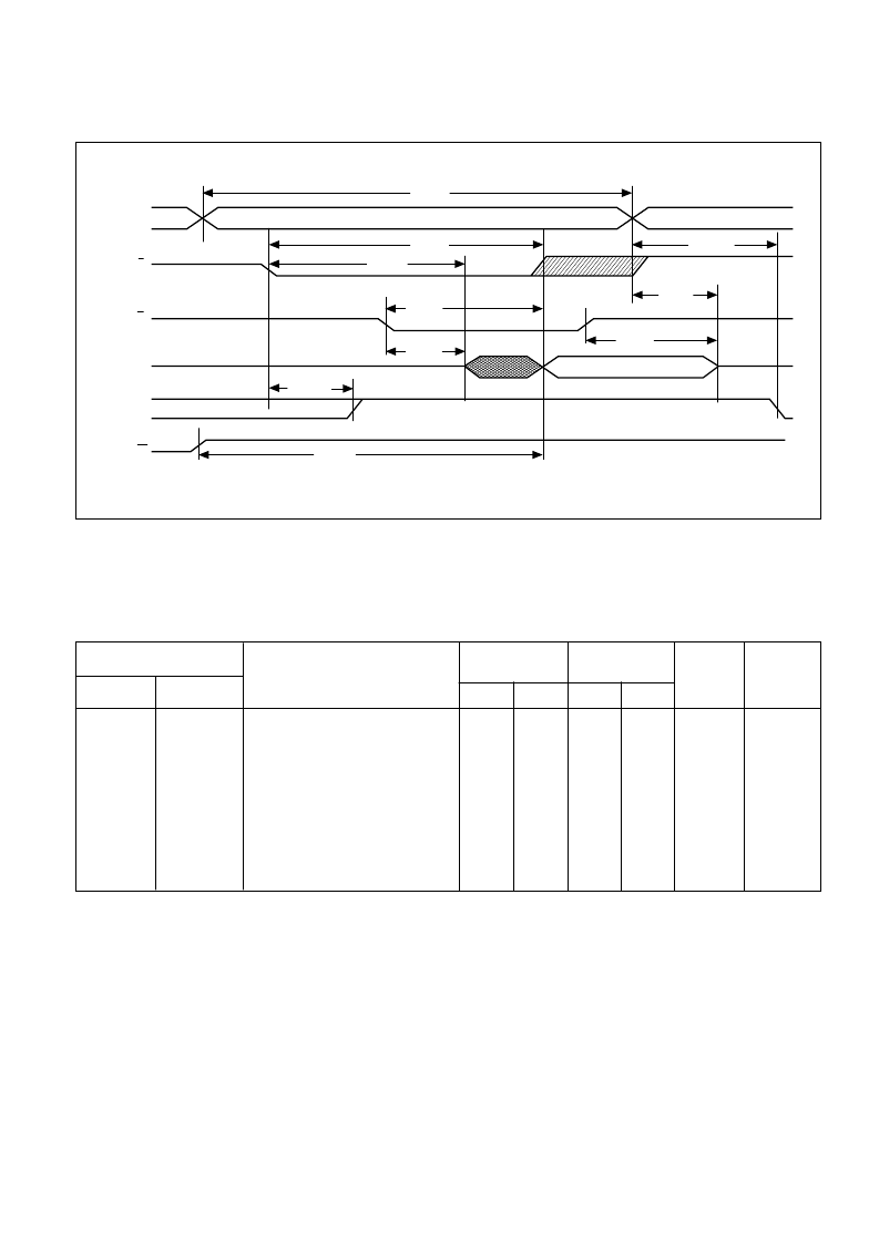
WRITE CYCLE 1 : W (BAR) CONTROLLED
(See notes 8 and 13)
Commercial and Industrial Temperature Range
t
WHQV
W
t
AVAV
t
ELQV
t
ELQX
t
EHICCL
t
EHQZ
t
GHQZ
t
GLQX
t
ELICCH
DATA VALID
STANDBY
ACTIVE
DQ (DATA OUT)
ADDRESS
E
G
I
CC
t
GLQV
F
igure 5. READ CYCLE 2 timing diagram (see note 9).
Standard
t
AVAV
t
WLWH
t
ELWH
t
DVWH
t
WHDX
t
AVWH
t
AVWL
t
WHAX
t
WLQZ
t
WHQZ
Alternative
t
WC
t
WP
t
CW
t
DW
t
DH
t
AW
t
AS
t
WR
t
WZ
t
OW
Parameter
Write cycle time
Write pulse width
Chip enable to end of write
Data set-up to end of write
Data hold after end of write
Address set-up to end of write
Address set-up to start of write
Address hold after end of write
Write enable to output disable
Output active after end of write
Units
ns
ns
ns
ns
ns
ns
ns
ns
ns
ns
Notes
11, 14
P10C68-45
P11C68-45
Min.
P10C68-35
P11C68-35
Min.
Symbol
45
35
35
30
0
35
0
0
5
Max.
35
45
35
35
30
0
35
0
0
5
Max.
35
NOTES
13.
14.
E (bar) or W (bar) must be
≥
VIH during address transitions.
If W (bar) is low when E (bar) goes low, the outputs remain in the high impedance state.
相關(guān)PDF資料 |
PDF描述 |
|---|---|
| P11C68-45DCBS | CMOS/SNOS NVSRAM HIGH PERFORMANCE 8 K x 8 NON-VOLATILE STATIC RAM |
| P11C68-45DPBS | CMOS/SNOS NVSRAM HIGH PERFORMANCE 8 K x 8 NON-VOLATILE STATIC RAM |
| P11C68-45IG | CMOS/SNOS NVSRAM HIGH PERFORMANCE 8 K x 8 NON-VOLATILE STATIC RAM |
| P11C68-45IGDCBS | CMOS/SNOS NVSRAM HIGH PERFORMANCE 8 K x 8 NON-VOLATILE STATIC RAM |
| P11C68-45IGDPBS | CMOS/SNOS NVSRAM HIGH PERFORMANCE 8 K x 8 NON-VOLATILE STATIC RAM |
相關(guān)代理商/技術(shù)參數(shù) |
參數(shù)描述 |
|---|---|
| P11C68-45DCBS | 制造商:ZARLINK 制造商全稱:Zarlink Semiconductor Inc 功能描述:CMOS/SNOS NVSRAM HIGH PERFORMANCE 8 K x 8 NON-VOLATILE STATIC RAM |
| P11C68-45DPBS | 制造商:ZARLINK 制造商全稱:Zarlink Semiconductor Inc 功能描述:CMOS/SNOS NVSRAM HIGH PERFORMANCE 8 K x 8 NON-VOLATILE STATIC RAM |
| P11C68-45IG | 制造商:ZARLINK 制造商全稱:Zarlink Semiconductor Inc 功能描述:CMOS/SNOS NVSRAM HIGH PERFORMANCE 8 K x 8 NON-VOLATILE STATIC RAM |
| P11C68-45IGDCBS | 制造商:ZARLINK 制造商全稱:Zarlink Semiconductor Inc 功能描述:CMOS/SNOS NVSRAM HIGH PERFORMANCE 8 K x 8 NON-VOLATILE STATIC RAM |
| P11C68-45IGDPBS | 制造商:ZARLINK 制造商全稱:Zarlink Semiconductor Inc 功能描述:CMOS/SNOS NVSRAM HIGH PERFORMANCE 8 K x 8 NON-VOLATILE STATIC RAM |
發(fā)布緊急采購,3分鐘左右您將得到回復。