- 您現(xiàn)在的位置:買賣IC網(wǎng) > PDF目錄384806 > OZ962R (Electronic Theatre Controls, Inc.) High-Efficiency Inverter Controller PDF資料下載
參數(shù)資料
| 型號: | OZ962R |
| 廠商: | Electronic Theatre Controls, Inc. |
| 英文描述: | High-Efficiency Inverter Controller |
| 中文描述: | 高效率逆變控制器 |
| 文件頁數(shù): | 4/6頁 |
| 文件大?。?/td> | 51K |
| 代理商: | OZ962R |
OZ962
OZ962-SF-2.7
Page 4
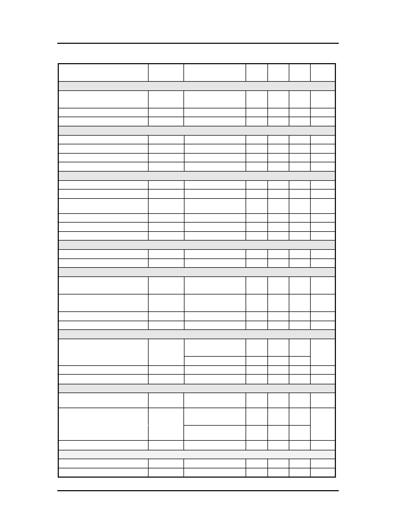
FUNCTIONAL SPECIFICATIONS
Parameter
Symbol
Test Conditions
5 V < VDD < 15 V
Limits
Typ
Unit
Min
Max
Reference Voltage
Nominal voltage
Vref
I
load
= 0.25 mA,
VDD = 5 V
2.37
2.50
2.63
V
Line regulation
Load regulation
I
load
= 0.2 mA to 1.0 mA
-
-
8
1
-
-
mV/V
mV/mA
Oscillator
Initial accuracy
Ramp peak
fosc
Ct = 220 pF, Rt = 120 k
48
2.45
53
2.55
58
2.65
KHz
V
Ramp valley
Temp. stability
TA = 0
o
C to 70
o
C
0.40
-
0.45
-
0.50
200
V
ppm/
o
C
Error Amplifier
Input bias current
Input offset voltage
V
ADJ
=V
FB
=2.0 V
V
FB
= 4.0 V
-
-
25
5
500
10
nA
mV
Input voltage range
0
-
VDD-
1.5
V
Open loop voltage gain
Unity gain bandwidth
50
1
60
1.5
-
-
dB
MHz
Power supply rejection
Under-Voltage Lockout
50
60
-
dB
Positive-going threshold voltage
-
3.8
4
V
Negative-going threshold voltage
Supply
3.4
3.6
-
V
Supply current - Enable Low
Adj, CT = Open
I
OFF
VDD
= 5.0 V
-
25
120
μ
A
Supply current - Enable Low
Adj, CT = Open
Supply current - Enable High
I
OFF
VDD
= 15 V
-
25
120
μ
A
I
ON
VDD
= 5.0 V
-
0.6
1.5
mA
Supply current - Enable High
NDR output
I
ON
VDD
= 15 V
-
0.6
1.5
mA
Output high voltage
V
OH
Isink = 10 mA,
VDD < 7.8 V
VDD >7.8 V
VDD-
0.3
VDD-
0.5
-
V
7.0
8.0
9.0
V
Output low voltage
Output resistance
V
OL
R
OUT
Isource = 10 mA
VDD
= 5.0 V
-
-
0.3
50
0.8
80
V
V
PDR output
Output high voltage
V
OH
Isink = 10 mA
VDD-
0.6
0.4
VDD-
0.3
0.5
-
Output low voltage
V
OL
Isource = 10 mA,
VDD < 7.8 V
VDD > 7.8 V
0.8
V
-
VDD-
6.0
50
VDD-
4.0
80
Output resistance
R
OUT
VDD
= 5.0 V
-
ns
Break-Before-Make
Qn off to Qp on delay
T
HL
200
240
280
Qp off to Qn on delay
T
LH
220
260
300
ns
相關(guān)PDF資料 |
PDF描述 |
|---|---|
| OZ965IG | High-Efficiency Inverter Controller |
| OZ965IR | High-Efficiency Inverter Controller |
| OZ965 | High-Efficiency Inverter Controller |
| OZ965G | High-Efficiency Inverter Controller |
| OZ965R | High-Efficiency Inverter Controller |
相關(guān)代理商/技術(shù)參數(shù) |
參數(shù)描述 |
|---|---|
| OZ964 | 制造商:未知廠家 制造商全稱:未知廠家 功能描述:Change Summary |
| OZ964D | 制造商:未知廠家 制造商全稱:未知廠家 功能描述:Change Summary |
| OZ964DN | 制造商:未知廠家 制造商全稱:未知廠家 功能描述:Change Summary |
| OZ964G | 制造商:未知廠家 制造商全稱:未知廠家 功能描述:Change Summary |
| OZ964GN | 制造商:未知廠家 制造商全稱:未知廠家 功能描述:Change Summary |
發(fā)布緊急采購,3分鐘左右您將得到回復(fù)。