- 您現(xiàn)在的位置:買(mǎi)賣(mài)IC網(wǎng) > PDF目錄11731 > ORT42G5-2BM484C (Lattice Semiconductor Corporation)IC FPSC TRANSCEIVER 4CH 484-BGA PDF資料下載
參數(shù)資料
| 型號(hào): | ORT42G5-2BM484C |
| 廠商: | Lattice Semiconductor Corporation |
| 文件頁(yè)數(shù): | 51/119頁(yè) |
| 文件大小: | 0K |
| 描述: | IC FPSC TRANSCEIVER 4CH 484-BGA |
| 產(chǎn)品變化通告: | Product Discontinuation 01/Aug/2011 |
| 標(biāo)準(zhǔn)包裝: | 60 |
| 系列: | * |
第1頁(yè)第2頁(yè)第3頁(yè)第4頁(yè)第5頁(yè)第6頁(yè)第7頁(yè)第8頁(yè)第9頁(yè)第10頁(yè)第11頁(yè)第12頁(yè)第13頁(yè)第14頁(yè)第15頁(yè)第16頁(yè)第17頁(yè)第18頁(yè)第19頁(yè)第20頁(yè)第21頁(yè)第22頁(yè)第23頁(yè)第24頁(yè)第25頁(yè)第26頁(yè)第27頁(yè)第28頁(yè)第29頁(yè)第30頁(yè)第31頁(yè)第32頁(yè)第33頁(yè)第34頁(yè)第35頁(yè)第36頁(yè)第37頁(yè)第38頁(yè)第39頁(yè)第40頁(yè)第41頁(yè)第42頁(yè)第43頁(yè)第44頁(yè)第45頁(yè)第46頁(yè)第47頁(yè)第48頁(yè)第49頁(yè)第50頁(yè)當(dāng)前第51頁(yè)第52頁(yè)第53頁(yè)第54頁(yè)第55頁(yè)第56頁(yè)第57頁(yè)第58頁(yè)第59頁(yè)第60頁(yè)第61頁(yè)第62頁(yè)第63頁(yè)第64頁(yè)第65頁(yè)第66頁(yè)第67頁(yè)第68頁(yè)第69頁(yè)第70頁(yè)第71頁(yè)第72頁(yè)第73頁(yè)第74頁(yè)第75頁(yè)第76頁(yè)第77頁(yè)第78頁(yè)第79頁(yè)第80頁(yè)第81頁(yè)第82頁(yè)第83頁(yè)第84頁(yè)第85頁(yè)第86頁(yè)第87頁(yè)第88頁(yè)第89頁(yè)第90頁(yè)第91頁(yè)第92頁(yè)第93頁(yè)第94頁(yè)第95頁(yè)第96頁(yè)第97頁(yè)第98頁(yè)第99頁(yè)第100頁(yè)第101頁(yè)第102頁(yè)第103頁(yè)第104頁(yè)第105頁(yè)第106頁(yè)第107頁(yè)第108頁(yè)第109頁(yè)第110頁(yè)第111頁(yè)第112頁(yè)第113頁(yè)第114頁(yè)第115頁(yè)第116頁(yè)第117頁(yè)第118頁(yè)第119頁(yè)
Lattice Semiconductor
ORCA ORT42G5 and ORT82G5 Data Sheet
37
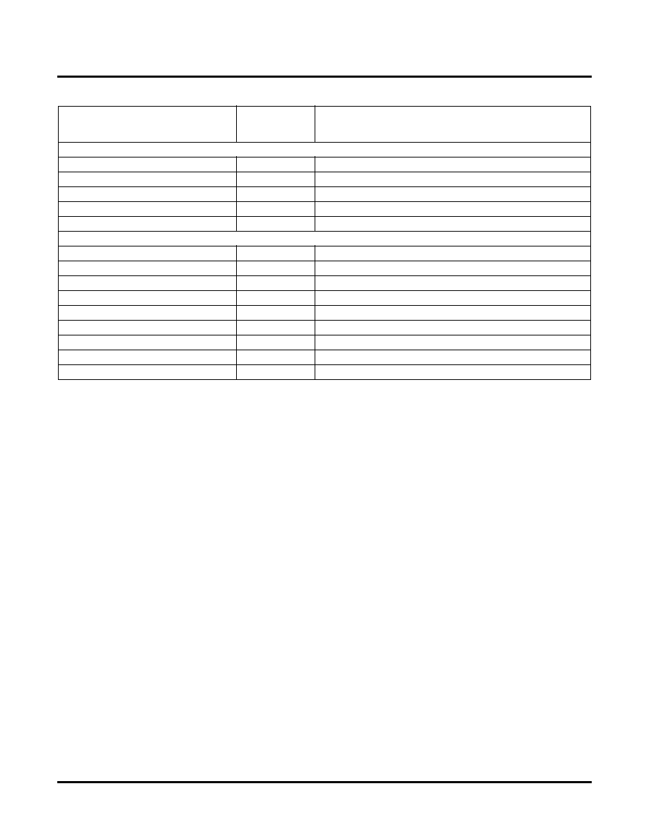
Table 12. Transceiver Embedded Core/FPGA Interface Signal Description for the ORT82G5
Reference Clocks and Internal Clock Distribution
Reference Clock Requirements
There are two pairs of reference clock inputs on the ORT42G5 and ORT82G5. The differential reference clock is
distributed to all channels in a block. Each channel has a differential buffer to isolate the clock from the other chan-
nels. The input clock is preferably a differential signal; however, the device can operate with a single-ended input.
The input reference clock directly impacts the transmit data eye, so the clock should have low jitter. In particular, jit-
ter components in the DC to 5 MHz range should be minimized. The required electrical characteristics for the refer-
ence clock are given in Table 38.
Note: In sections of this data sheet, the differential clocks are simply referred to as the reference clock as
REFCLK_[A:B].
Synthesized and Recovered Clocks
The SERDES Embedded Core block contains its own dedicated PLLs for transmit and receive clock generation.
The user provides a reference clock of the appropriate frequency, as described in the previous section. The trans-
mitter PLL uses the REFCLK_[A,B] inputs to synthesize the internal high-speed serial bit clocks. The receiver PLLs
extract the clock from the serial input data and retime the data with the recovered clock.
The receive PLL for each channel has two modes of operation - lock to reference and lock to data with retiming.
When no data or invalid data is present on the HDINP_xx and HDINN_xx pins, the receive VCO will not lock to data
and its frequency can drift outside of the nominal ±350 ppm range. Under this condition, the receive PLL will lock to
REFCLK_[A,B] for a xed time interval and then will attempt to lock to receive data. The process of attempting to
lock to data, then locking to clock will repeat until valid input data exists. There is also a control register bit per
channel to force the receive PLL to always lock to the reference clock.
The high-speed transmit and receive serial data links can run at 0.6 to 3.7 Gbps, depending on the frequency of the
reference clock and the state of the control bits from the internal transmit control register. The interface to the seri-
alizer/deserializer block runs at 1/10th the bit rate of the data lane. Additionally, the MUX/DEMUX logic converts the
FPGA/Embedded Core
Interface Signal Name
xx=... line remain (xx = [AA, ..., BD]
Input (I) to or
Output (O) from
Core
Signal Description
Transmit Path Signals
TWDxx[31:0]
I
Transmit data – channel xx.
TCOMMAxx[3:0]
I
Transmit comma character – channel xx.
TBIT9xx[3:0]
I
Transmit force negative disparity – channel xx
TSYS_CLK_xx
I
Transmit low-speed clock to the FPGA – channel xx
TCK78[A:B]
O
Transmit low-speed clock to the FPGA – SERDES Quad [A:B].
Receive Path Signals
MRWDxx[39:0]
O
RWCKxx
O
Low-speed receive clock—Channel xx.
RCK78[A:B]
O
Receive low-speed clock to FPGA—SERDES Quad [A:B].
RSYS_CLK_A1
I
Low-speed receive FIFO clock for channels AA, AB
RSYS_CLK_A2
I
Low-speed receive FIFO clock for channels AC, AD
RSYS_CLK_B1
I
Low-speed receive FIFO clock for channels BA, BB
RSYS_CLK_B2
I
Low-speed receive FIFO clock for channels BC, BD
CV_SELxx
I
Enable detection of code violations in the incoming data
SYS_RST_N
I
Synchronous reset of the channel alignment blocks.
相關(guān)PDF資料 |
PDF描述 |
|---|---|
| ORT42G5-1BM484I | IC FPSC TRANSCEIVER 4CH 484-BGA |
| GRM1885C1H561JA01D | CAP CER 560PF 50V 5% NP0 0603 |
| ORT42G5-1BM484C | IC FPSC TRANSCEIVER 4CH 484-BGA |
| PIC17C43-25/P | IC MCU OTP 4KX16 PWM 40DIP |
| ORSO82G5-2F680I | IC FPSC TRANSCEIVER 8CH 680-BGA |
相關(guān)代理商/技術(shù)參數(shù) |
參數(shù)描述 |
|---|---|
| ORT42G5-2BM484I | 功能描述:FPGA - 現(xiàn)場(chǎng)可編程門(mén)陣列 10368 LUT 204 I/O RoHS:否 制造商:Altera Corporation 系列:Cyclone V E 柵極數(shù)量: 邏輯塊數(shù)量:943 內(nèi)嵌式塊RAM - EBR:1956 kbit 輸入/輸出端數(shù)量:128 最大工作頻率:800 MHz 工作電源電壓:1.1 V 最大工作溫度:+ 70 C 安裝風(fēng)格:SMD/SMT 封裝 / 箱體:FBGA-256 |
| ORT42G5-2BMN484C | 功能描述:FPGA - 現(xiàn)場(chǎng)可編程門(mén)陣列 10368 LUT 204 I/O RoHS:否 制造商:Altera Corporation 系列:Cyclone V E 柵極數(shù)量: 邏輯塊數(shù)量:943 內(nèi)嵌式塊RAM - EBR:1956 kbit 輸入/輸出端數(shù)量:128 最大工作頻率:800 MHz 工作電源電壓:1.1 V 最大工作溫度:+ 70 C 安裝風(fēng)格:SMD/SMT 封裝 / 箱體:FBGA-256 |
| ORT42G5-2BMN484I | 功能描述:FPGA - 現(xiàn)場(chǎng)可編程門(mén)陣列 10368 LUT 204 I/O RoHS:否 制造商:Altera Corporation 系列:Cyclone V E 柵極數(shù)量: 邏輯塊數(shù)量:943 內(nèi)嵌式塊RAM - EBR:1956 kbit 輸入/輸出端數(shù)量:128 最大工作頻率:800 MHz 工作電源電壓:1.1 V 最大工作溫度:+ 70 C 安裝風(fēng)格:SMD/SMT 封裝 / 箱體:FBGA-256 |
| ORT42G5-3BM484C | 功能描述:FPGA - 現(xiàn)場(chǎng)可編程門(mén)陣列 10368 LUT 204 I/O RoHS:否 制造商:Altera Corporation 系列:Cyclone V E 柵極數(shù)量: 邏輯塊數(shù)量:943 內(nèi)嵌式塊RAM - EBR:1956 kbit 輸入/輸出端數(shù)量:128 最大工作頻率:800 MHz 工作電源電壓:1.1 V 最大工作溫度:+ 70 C 安裝風(fēng)格:SMD/SMT 封裝 / 箱體:FBGA-256 |
| ORT42G5-3BMN484C | 功能描述:FPGA - 現(xiàn)場(chǎng)可編程門(mén)陣列 10368 LUT 204 I/O RoHS:否 制造商:Altera Corporation 系列:Cyclone V E 柵極數(shù)量: 邏輯塊數(shù)量:943 內(nèi)嵌式塊RAM - EBR:1956 kbit 輸入/輸出端數(shù)量:128 最大工作頻率:800 MHz 工作電源電壓:1.1 V 最大工作溫度:+ 70 C 安裝風(fēng)格:SMD/SMT 封裝 / 箱體:FBGA-256 |
發(fā)布緊急采購(gòu),3分鐘左右您將得到回復(fù)。