- 您現在的位置:買賣IC網 > PDF目錄299576 > OR3T165-5B432 FPGA, 1024 CLBS, 120000 GATES, PBGA432 PDF資料下載
參數資料
| 型號: | OR3T165-5B432 |
| 元件分類: | FPGA |
| 英文描述: | FPGA, 1024 CLBS, 120000 GATES, PBGA432 |
| 封裝: | BGA-432 |
| 文件頁數: | 187/210頁 |
| 文件大小: | 2138K |
| 代理商: | OR3T165-5B432 |
第1頁第2頁第3頁第4頁第5頁第6頁第7頁第8頁第9頁第10頁第11頁第12頁第13頁第14頁第15頁第16頁第17頁第18頁第19頁第20頁第21頁第22頁第23頁第24頁第25頁第26頁第27頁第28頁第29頁第30頁第31頁第32頁第33頁第34頁第35頁第36頁第37頁第38頁第39頁第40頁第41頁第42頁第43頁第44頁第45頁第46頁第47頁第48頁第49頁第50頁第51頁第52頁第53頁第54頁第55頁第56頁第57頁第58頁第59頁第60頁第61頁第62頁第63頁第64頁第65頁第66頁第67頁第68頁第69頁第70頁第71頁第72頁第73頁第74頁第75頁第76頁第77頁第78頁第79頁第80頁第81頁第82頁第83頁第84頁第85頁第86頁第87頁第88頁第89頁第90頁第91頁第92頁第93頁第94頁第95頁第96頁第97頁第98頁第99頁第100頁第101頁第102頁第103頁第104頁第105頁第106頁第107頁第108頁第109頁第110頁第111頁第112頁第113頁第114頁第115頁第116頁第117頁第118頁第119頁第120頁第121頁第122頁第123頁第124頁第125頁第126頁第127頁第128頁第129頁第130頁第131頁第132頁第133頁第134頁第135頁第136頁第137頁第138頁第139頁第140頁第141頁第142頁第143頁第144頁第145頁第146頁第147頁第148頁第149頁第150頁第151頁第152頁第153頁第154頁第155頁第156頁第157頁第158頁第159頁第160頁第161頁第162頁第163頁第164頁第165頁第166頁第167頁第168頁第169頁第170頁第171頁第172頁第173頁第174頁第175頁第176頁第177頁第178頁第179頁第180頁第181頁第182頁第183頁第184頁第185頁第186頁當前第187頁第188頁第189頁第190頁第191頁第192頁第193頁第194頁第195頁第196頁第197頁第198頁第199頁第200頁第201頁第202頁第203頁第204頁第205頁第206頁第207頁第208頁第209頁第210頁
Preliminary Data Sheet, Rev. 1
ORCA Series 3 FPGAs
September 1998
78
Lucent Technologies Inc.
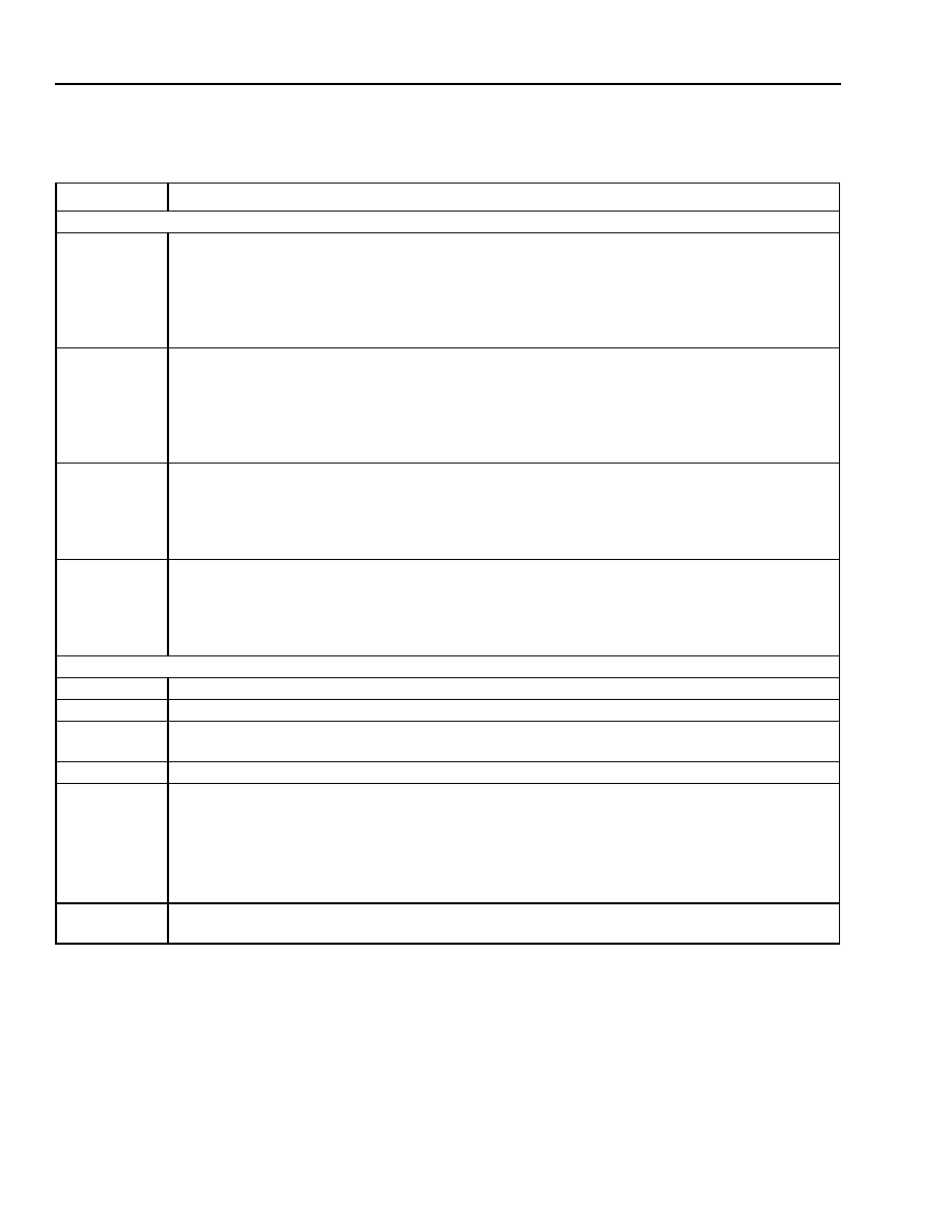
Register 6—Clock Source Status/Output Clock Selection Programming
Bits [1:0]
Read Only. These bits are set up via the configuration bit stream to indicate the input clock
source to the PCM. Default is clock input tied low (00).
00: clock input tied low
01: ExpressCLK corner pad
10: general routing
11: general routing
Bits [3:2]
Read Only. These bits are set up via the configuration bit stream to indicate the feedback clock
source to the PCM. Default is 00.
00: ExpressCLK dedicated feedback path
01: general routing
10: general routing
11: general routing
Bits [5:4]
ExpressCLK
Output Source Selector. Default is 00.
00: PCM input clock, bypass path through PCM
01: DLL output
10: tapped delay line output
11: divided (DIV2) delay line output
Bits [7:6]
System Clock Output Source Selector. Default is 00.
00: PCM input clock, bypass path through PCM
01: DLL output
10: tapped delay line output
11: reserved
Register 7—PCM Control Programming
Bit 0
PCM Analog Power Supply Switch. 1 = power supply on, 0 = power supply off.
Bit 1
PCM
Reset. A value of 1 resets all PCM logic for PLL and DLL modes.
Bit 2
DLL Reset. A value of 1 resets the clock generation logic for DLL mode. No dividers or user reg-
isters are affected.
Bits [5:3]
Reserved.
Bit 6
PCM
Configuration Operation Enable Bit. 0 = normal configuration operation. During configu-
ration (DONE = 0), the PCM analog power supply will be off, the PCM output data bus is 3-stated,
and the LOCK signal is asserted to logic 0. The PCM will power up when DONE = 1.
1 = PCM operation during configuration. The PCM may be powered up (see bit 0) and begin
operation, or continue operation. The setup of the PCM can be performed via the configuration
bit stream.
Bit 7
PCM GSRN Enable Bit. 0 = normal GSRN operation. 1 = GSRN has no effect on PCM logic, so
clock processing will not be interrupted by a chip reset. Default is 0.
Programmable Clock Manager (PCM): Advance Information (continued)
Table 30. PCM Control Registers (continued)
Bit #
Function
相關PDF資料 |
PDF描述 |
|---|---|
| OR3T165-5B600 | FPGA, 1024 CLBS, 120000 GATES, PBGA600 |
| OR3T165-5BA352I | FPGA, 1024 CLBS, 120000 GATES, PBGA352 |
| OR3T165-5BA352 | FPGA, 1024 CLBS, 120000 GATES, PBGA352 |
| OR3T165-5BC432I | FPGA, 1024 CLBS, 120000 GATES, PBGA432 |
| OR3T165-5BC600I | FPGA, 1024 CLBS, 120000 GATES, PBGA600 |
相關代理商/技術參數 |
參數描述 |
|---|---|
| OR3T20 | 制造商:AGERE 制造商全稱:AGERE 功能描述:3C and 3T Field-Programmable Gate Arrays |
| OR3T20-4BA256I | 制造商:未知廠家 制造商全稱:未知廠家 功能描述:Field Programmable Gate Array (FPGA) |
| OR3T20-4S208I | 制造商:未知廠家 制造商全稱:未知廠家 功能描述:Field Programmable Gate Array (FPGA) |
| OR3T20-4S240I | 制造商:未知廠家 制造商全稱:未知廠家 功能描述:Field Programmable Gate Array (FPGA) |
| OR3T20-5BA256 | 制造商:AGERE 制造商全稱:AGERE 功能描述:3C and 3T Field-Programmable Gate Arrays |
發(fā)布緊急采購,3分鐘左右您將得到回復。