- 您現(xiàn)在的位置:買(mǎi)賣(mài)IC網(wǎng) > PDF目錄299576 > OR3T125-4BC600I FPGA, 784 CLBS, 92000 GATES, 80 MHz, PBGA600 PDF資料下載
參數(shù)資料
| 型號(hào): | OR3T125-4BC600I |
| 元件分類(lèi): | FPGA |
| 英文描述: | FPGA, 784 CLBS, 92000 GATES, 80 MHz, PBGA600 |
| 封裝: | BGA-600 |
| 文件頁(yè)數(shù): | 13/210頁(yè) |
| 文件大?。?/td> | 2138K |
| 代理商: | OR3T125-4BC600I |
第1頁(yè)第2頁(yè)第3頁(yè)第4頁(yè)第5頁(yè)第6頁(yè)第7頁(yè)第8頁(yè)第9頁(yè)第10頁(yè)第11頁(yè)第12頁(yè)當(dāng)前第13頁(yè)第14頁(yè)第15頁(yè)第16頁(yè)第17頁(yè)第18頁(yè)第19頁(yè)第20頁(yè)第21頁(yè)第22頁(yè)第23頁(yè)第24頁(yè)第25頁(yè)第26頁(yè)第27頁(yè)第28頁(yè)第29頁(yè)第30頁(yè)第31頁(yè)第32頁(yè)第33頁(yè)第34頁(yè)第35頁(yè)第36頁(yè)第37頁(yè)第38頁(yè)第39頁(yè)第40頁(yè)第41頁(yè)第42頁(yè)第43頁(yè)第44頁(yè)第45頁(yè)第46頁(yè)第47頁(yè)第48頁(yè)第49頁(yè)第50頁(yè)第51頁(yè)第52頁(yè)第53頁(yè)第54頁(yè)第55頁(yè)第56頁(yè)第57頁(yè)第58頁(yè)第59頁(yè)第60頁(yè)第61頁(yè)第62頁(yè)第63頁(yè)第64頁(yè)第65頁(yè)第66頁(yè)第67頁(yè)第68頁(yè)第69頁(yè)第70頁(yè)第71頁(yè)第72頁(yè)第73頁(yè)第74頁(yè)第75頁(yè)第76頁(yè)第77頁(yè)第78頁(yè)第79頁(yè)第80頁(yè)第81頁(yè)第82頁(yè)第83頁(yè)第84頁(yè)第85頁(yè)第86頁(yè)第87頁(yè)第88頁(yè)第89頁(yè)第90頁(yè)第91頁(yè)第92頁(yè)第93頁(yè)第94頁(yè)第95頁(yè)第96頁(yè)第97頁(yè)第98頁(yè)第99頁(yè)第100頁(yè)第101頁(yè)第102頁(yè)第103頁(yè)第104頁(yè)第105頁(yè)第106頁(yè)第107頁(yè)第108頁(yè)第109頁(yè)第110頁(yè)第111頁(yè)第112頁(yè)第113頁(yè)第114頁(yè)第115頁(yè)第116頁(yè)第117頁(yè)第118頁(yè)第119頁(yè)第120頁(yè)第121頁(yè)第122頁(yè)第123頁(yè)第124頁(yè)第125頁(yè)第126頁(yè)第127頁(yè)第128頁(yè)第129頁(yè)第130頁(yè)第131頁(yè)第132頁(yè)第133頁(yè)第134頁(yè)第135頁(yè)第136頁(yè)第137頁(yè)第138頁(yè)第139頁(yè)第140頁(yè)第141頁(yè)第142頁(yè)第143頁(yè)第144頁(yè)第145頁(yè)第146頁(yè)第147頁(yè)第148頁(yè)第149頁(yè)第150頁(yè)第151頁(yè)第152頁(yè)第153頁(yè)第154頁(yè)第155頁(yè)第156頁(yè)第157頁(yè)第158頁(yè)第159頁(yè)第160頁(yè)第161頁(yè)第162頁(yè)第163頁(yè)第164頁(yè)第165頁(yè)第166頁(yè)第167頁(yè)第168頁(yè)第169頁(yè)第170頁(yè)第171頁(yè)第172頁(yè)第173頁(yè)第174頁(yè)第175頁(yè)第176頁(yè)第177頁(yè)第178頁(yè)第179頁(yè)第180頁(yè)第181頁(yè)第182頁(yè)第183頁(yè)第184頁(yè)第185頁(yè)第186頁(yè)第187頁(yè)第188頁(yè)第189頁(yè)第190頁(yè)第191頁(yè)第192頁(yè)第193頁(yè)第194頁(yè)第195頁(yè)第196頁(yè)第197頁(yè)第198頁(yè)第199頁(yè)第200頁(yè)第201頁(yè)第202頁(yè)第203頁(yè)第204頁(yè)第205頁(yè)第206頁(yè)第207頁(yè)第208頁(yè)第209頁(yè)第210頁(yè)
Lucent Technologies Inc.
11
Preliminary Data Sheet, Rev. 1
September 1998
ORCA Series 3 FPGAs
Programmable Logic Cells (continued)
Table 4. Control Input Functionality
Mode
CLK
LSR
CE
ASWE
SEL
Logic
CLK to all latches/
FFs
LSR to all latches/
FFs, enabled per nib-
ble and for ninth FF
CE to all latches/FFs,
selectable per nibble
and for ninth FF
CE to all latches/FFs,
selectable per nibble
and for ninth FF
Select between LUT
input and direct input
for eight latches/FFs
Half Logic/
Half Ripple
CLK to all latches/
FFs
LSR to all latches/FF,
enabled per nibble
and for ninth FF
CE to all latches/FFs,
selectable per nibble
and for ninth FF
Ripple logic control
input
Select between LUT
input and direct input
for eight latches/FFs
Ripple
CLK to all latches/
FFs
LSR to all latches/
FFs, enabled per nib-
ble and for ninth FF
CE to all latches/FFs,
selectable per nibble
and for ninth FF
Ripple logic control
input
Select between LUT
input and direct input
for eight latches/FFs
Memory
(RAM)
CLK to RAM
Port enable 2
Port enable 1
Write enable
Not used
Memory
(ROM)
Optional for sync.
outputs
Not used
Logic Mode
The PFU diagram of Figure 3 represents the logic
mode of operation. In logic mode, the eight LUTs are
used individually or in flexible groups to implement user
logic functions. The latches/FFs may be used in con-
junction with the LUTs or separately with the direct PFU
data inputs. There are three basic submodes of LUT
operation in PFU logic mode: F4 mode, F5 mode, and
softwired LUT (SWL) mode. Combinations of these
submodes are possible in each PFU.
F4 mode, shown simplified in Figure 4, illustrates the
uses of the basic 4-input LUTs in the PFU. The output
of an F4 LUT can be passed out of the PFU, captured
at the LUTs associated latch/FF, or multiplexed with the
adjacent F4 LUT output using one of the F5[A:D] inputs
to the PFU. Only adjacent LUT pairs (K0 and K1, K2
and K3, K4 and K5, K6 and K7) can be multiplexed, and
the output always goes to the even-numbered output of
the pair.
The F5 submode of the LUT operation, shown simpli-
fied in Figure 4, indicates the use of 5-input LUTs to
implement logic. 5-input LUTs are created from two
4-input LUTs and a multiplexer. The F5 LUT is the
same as the multiplexing of two F4 LUTs described
previously with the constraint that the inputs to the F4
LUTs be the same. The F5[A:D] input is then used as
the fifth LUT input. The equations for the two F4 LUTs
will differ by the assumed value for the F5[A:D] input,
one F4 LUT assuming that the F5[A:D] input is zero,
and the other assuming it is a one. The selection of the
appropriate F4 LUT output in the F5 MUX by the
F5[A:D] signal creates a 5-input LUT. Any combination
of F4 and F5 LUTs is allowed per PFU using the eight
16-bit LUTs. Examples are eight F4 LUTs, four F5
LUTs, and a combination of four F4 plus two F5 LUTs.
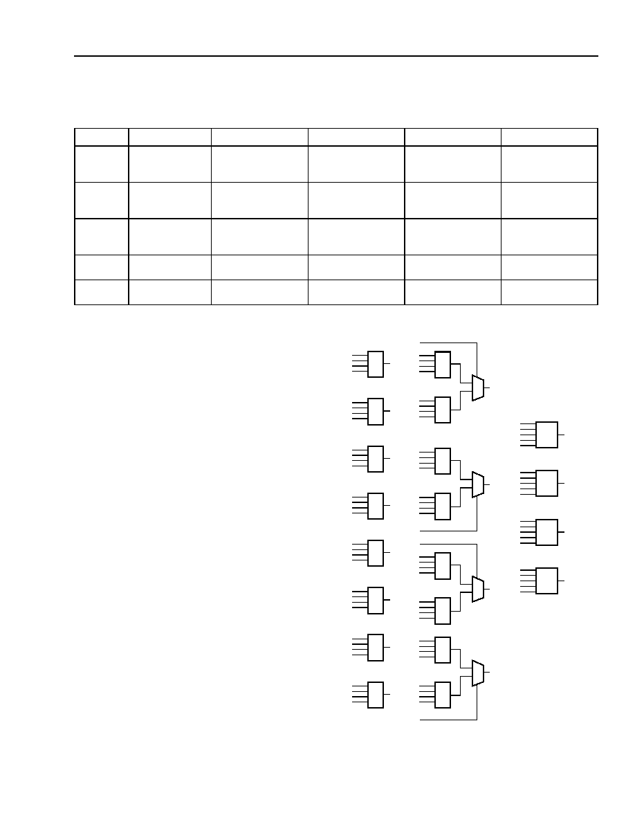
Figure 4. Simplified F4 and F5 Logic Modes
K7
F7
K7
F6
K6
F5D
K6
F6
K5
F5
K5
F4
K4
F5C
K4
F4
K3
F3
K3
F2
K2
F5B
K2
F2
K1
F1
K1
F0
K0
F5A
K0
F0
K7/K6
F6
K5/K4
F4
K3/K2
F2
K1/K0
F0
F5 MODE
MULTIPLEXED F4 MODE
F4 MODE
5-5970(F)
相關(guān)PDF資料 |
PDF描述 |
|---|---|
| OR3T80-4BC600I | FPGA, 484 CLBS, 58000 GATES, 80 MHz, PBGA600 |
| OR3T80-5BC600I | FPGA, 484 CLBS, 58000 GATES, 80 MHz, PBGA600 |
| OR3T80-6BC600I | FPGA, 484 CLBS, 58000 GATES, 80 MHz, PBGA600 |
| OR3T125-4PS208I | FPGA, 784 CLBS, 92000 GATES, 80 MHz, PQFP208 |
| OR3T125-4PS208 | FPGA, 784 CLBS, 92000 GATES, 80 MHz, PQFP208 |
相關(guān)代理商/技術(shù)參數(shù) |
參數(shù)描述 |
|---|---|
| OR3T125-4PS208I | 制造商:未知廠(chǎng)家 制造商全稱(chēng):未知廠(chǎng)家 功能描述:Field Programmable Gate Array (FPGA) |
| OR3T125-4PS240I | 制造商:未知廠(chǎng)家 制造商全稱(chēng):未知廠(chǎng)家 功能描述:Field Programmable Gate Array (FPGA) |
| OR3T125-5BA352 | 制造商:AGERE 制造商全稱(chēng):AGERE 功能描述:3C and 3T Field-Programmable Gate Arrays |
| OR3T125-5BA352I | 制造商:AGERE 制造商全稱(chēng):AGERE 功能描述:3C and 3T Field-Programmable Gate Arrays |
| OR3T125-5BC432 | 制造商:AGERE 制造商全稱(chēng):AGERE 功能描述:3C and 3T Field-Programmable Gate Arrays |
發(fā)布緊急采購(gòu),3分鐘左右您將得到回復(fù)。