- 您現(xiàn)在的位置:買賣IC網(wǎng) > PDF目錄383714 > OR2T04A-5S84 (Electronic Theatre Controls, Inc.) Field-Programmable Gate Arrays PDF資料下載
參數(shù)資料
| 型號: | OR2T04A-5S84 |
| 廠商: | Electronic Theatre Controls, Inc. |
| 元件分類: | FPGA |
| 英文描述: | Field-Programmable Gate Arrays |
| 中文描述: | 現(xiàn)場可編程門陣列 |
| 文件頁數(shù): | 28/192頁 |
| 文件大?。?/td> | 3148K |
| 代理商: | OR2T04A-5S84 |
第1頁第2頁第3頁第4頁第5頁第6頁第7頁第8頁第9頁第10頁第11頁第12頁第13頁第14頁第15頁第16頁第17頁第18頁第19頁第20頁第21頁第22頁第23頁第24頁第25頁第26頁第27頁當(dāng)前第28頁第29頁第30頁第31頁第32頁第33頁第34頁第35頁第36頁第37頁第38頁第39頁第40頁第41頁第42頁第43頁第44頁第45頁第46頁第47頁第48頁第49頁第50頁第51頁第52頁第53頁第54頁第55頁第56頁第57頁第58頁第59頁第60頁第61頁第62頁第63頁第64頁第65頁第66頁第67頁第68頁第69頁第70頁第71頁第72頁第73頁第74頁第75頁第76頁第77頁第78頁第79頁第80頁第81頁第82頁第83頁第84頁第85頁第86頁第87頁第88頁第89頁第90頁第91頁第92頁第93頁第94頁第95頁第96頁第97頁第98頁第99頁第100頁第101頁第102頁第103頁第104頁第105頁第106頁第107頁第108頁第109頁第110頁第111頁第112頁第113頁第114頁第115頁第116頁第117頁第118頁第119頁第120頁第121頁第122頁第123頁第124頁第125頁第126頁第127頁第128頁第129頁第130頁第131頁第132頁第133頁第134頁第135頁第136頁第137頁第138頁第139頁第140頁第141頁第142頁第143頁第144頁第145頁第146頁第147頁第148頁第149頁第150頁第151頁第152頁第153頁第154頁第155頁第156頁第157頁第158頁第159頁第160頁第161頁第162頁第163頁第164頁第165頁第166頁第167頁第168頁第169頁第170頁第171頁第172頁第173頁第174頁第175頁第176頁第177頁第178頁第179頁第180頁第181頁第182頁第183頁第184頁第185頁第186頁第187頁第188頁第189頁第190頁第191頁第192頁
28
Lucent Technologies Inc.
Data Sheet
June 1999
ORCA Series 2 FPGAs
Programmable Input/Output Cells
(continued)
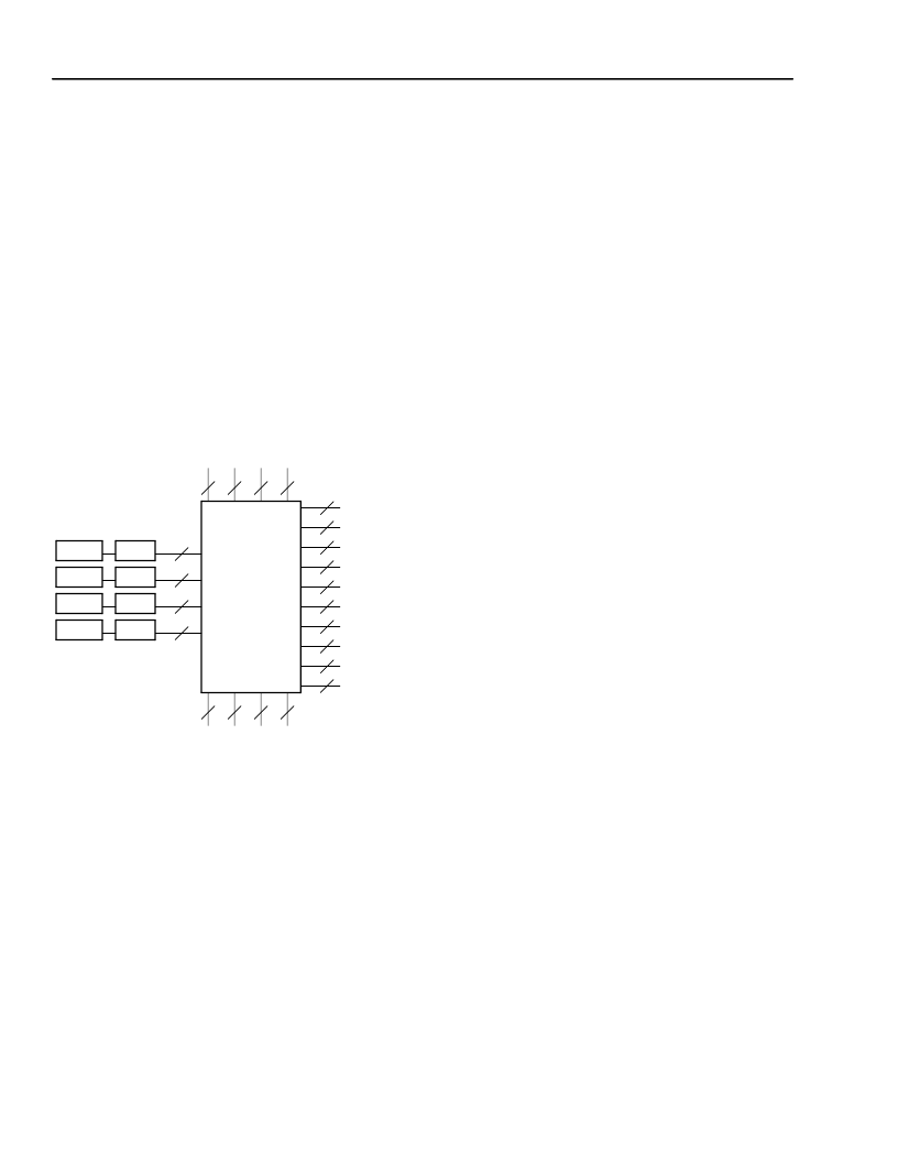
PIC Routing Resources
The PIC routing is designed to route 4-bit wide buses
efficiently. For example, any four consecutive I/O pads
can have both their input and output signals routed into
one PLC. Using only PIC routing, either the input or
output data can be routed to/from a single PLC from/to
any eight pads in a row, as in Figure 25.
The connections between PLCs and the I/O pad are
provided by two basic types of routing resources.
These are routing resources internal to the PIC and
routing resources used for PIC-PLC connection.
Figure 26 and Figure 27 show a high-level and detailed
view of these routing resources, respectively.
5-4504(F)
Figure 25. Simplified PIC Routing Diagram
The PIC’s name is represented by a two-letter designa-
tion to indicate on which side of the device it is located
followed by a number to indicate in which row or col-
umn it is located. The first letter, P designates that the
cell is a PIC and not a PLC. The second letter indicates
the side of the array where the PIC is located. The four
sides are left (L), right (R), top (T), and bottom (B). The
individual I/O pad is indicated by a single letter (either
A, B, C, or D) placed at the end of the PIC name. As an
example, PL10A indicates a pad located on the left
side of the array in the tenth row.
Each PIC has four pads and each pad can be config-
ured as an input, an output (3-statable), a direct output,
or a bidirectional I/O. When the pads are used as
inputs, the external signals are provided to the internal
circuitry at IN[3:0]. When the pads are used to provide
direct inputs to the latches/FFs, they are connected
through DIN[3:0]. When the pads are used as outputs,
the internal signals connect to the pads through
OUT[3:0]. When the pads are used as direct outputs,
the output from the latches/flip-flops in the PLCs to the
PIC is designated DOUT[3:0]. When the outputs are
3-statable, the 3-state enable signals are TS[3:0].
Routing Resources Internal to the PIC
For inter-PIC routing, the PIC contains 14 lines used to
route signals around the perimeter of the FPGA. Figure
25 shows these lines running vertically for a PIC
located on the left side. Figure 26 shows the lines run-
ning horizontally for a PIC located at the top of the
FPGA.
PXL Lines.
Each PIC has two PXL lines, labeled
PXL[1:0]. Like the XL lines of the PLC, the PXL lines
span the entire edge of the FPGA.
PXH Lines.
Each PIC has four PXH lines, labeled
PXH[3:0]. Like the XH lines of the PLC, the PXH lines
span half the edge of the FPGA.
PX2 Lines.
There are four PX2 lines in each PIC,
labeled PX2[3:0]. The PX2 lines pass through two adja-
cent PICs before being broken. These are used to
route nets around the perimeter equally a distance of
two or more PICs.
PX1 Lines.
Each PIC has four PX1 lines, labeled
PX1[3:0]. The PX1 lines are one PIC long and are
extended to adjacent PICs by enabling CIPs.
PAD D
I/O3
4
PXL
2
CK
2
PIC
SWITCHING
MATRIX
PAD C
I/O2
4
PAD B
I/O1
4
PAD A
I/O0
4
PXH
4
PX2
4
PX1
4
PLC X4
4
PLC X1
4
PLC PSW
5
PLC DOUT
4
PLC XL
4
PLC XH
4
PLC X1
4
PLC X4
4
PLC DIN
4
PXL
2
PXH
4
PX2
4
PX1
4
相關(guān)PDF資料 |
PDF描述 |
|---|---|
| OR2T04A-5S84I | Field-Programmable Gate Arrays |
| OR2T04A-5T208 | Field-Programmable Gate Arrays |
| OR2T04A-5T208I | Field-Programmable Gate Arrays |
| OR2T04A-5T84 | Field-Programmable Gate Arrays |
| OR2T04A-5T84I | Field-Programmable Gate Arrays |
相關(guān)代理商/技術(shù)參數(shù) |
參數(shù)描述 |
|---|---|
| OR2T04A-5S84I | 制造商:未知廠家 制造商全稱:未知廠家 功能描述:Field-Programmable Gate Arrays |
| OR2T04A-5T100 | 制造商:未知廠家 制造商全稱:未知廠家 功能描述:Field-Programmable Gate Arrays |
| OR2T04A5T100-DB | 功能描述:FPGA - 現(xiàn)場可編程門陣列 400 LUT 152 I/O RoHS:否 制造商:Altera Corporation 系列:Cyclone V E 柵極數(shù)量: 邏輯塊數(shù)量:943 內(nèi)嵌式塊RAM - EBR:1956 kbit 輸入/輸出端數(shù)量:128 最大工作頻率:800 MHz 工作電源電壓:1.1 V 最大工作溫度:+ 70 C 安裝風(fēng)格:SMD/SMT 封裝 / 箱體:FBGA-256 |
| OR2T04A-5T100I | 制造商:未知廠家 制造商全稱:未知廠家 功能描述:Field-Programmable Gate Arrays |
| OR2T04A-5T144 | 制造商:未知廠家 制造商全稱:未知廠家 功能描述:Field-Programmable Gate Arrays |
發(fā)布緊急采購,3分鐘左右您將得到回復(fù)。