- 您現(xiàn)在的位置:買賣IC網(wǎng) > PDF目錄383708 > OR2T04A-3T160I (Electronic Theatre Controls, Inc.) Field-Programmable Gate Arrays PDF資料下載
參數(shù)資料
| 型號: | OR2T04A-3T160I |
| 廠商: | Electronic Theatre Controls, Inc. |
| 元件分類: | FPGA |
| 英文描述: | Field-Programmable Gate Arrays |
| 中文描述: | 現(xiàn)場可編程門陣列 |
| 文件頁數(shù): | 66/192頁 |
| 文件大?。?/td> | 3148K |
| 代理商: | OR2T04A-3T160I |
第1頁第2頁第3頁第4頁第5頁第6頁第7頁第8頁第9頁第10頁第11頁第12頁第13頁第14頁第15頁第16頁第17頁第18頁第19頁第20頁第21頁第22頁第23頁第24頁第25頁第26頁第27頁第28頁第29頁第30頁第31頁第32頁第33頁第34頁第35頁第36頁第37頁第38頁第39頁第40頁第41頁第42頁第43頁第44頁第45頁第46頁第47頁第48頁第49頁第50頁第51頁第52頁第53頁第54頁第55頁第56頁第57頁第58頁第59頁第60頁第61頁第62頁第63頁第64頁第65頁當(dāng)前第66頁第67頁第68頁第69頁第70頁第71頁第72頁第73頁第74頁第75頁第76頁第77頁第78頁第79頁第80頁第81頁第82頁第83頁第84頁第85頁第86頁第87頁第88頁第89頁第90頁第91頁第92頁第93頁第94頁第95頁第96頁第97頁第98頁第99頁第100頁第101頁第102頁第103頁第104頁第105頁第106頁第107頁第108頁第109頁第110頁第111頁第112頁第113頁第114頁第115頁第116頁第117頁第118頁第119頁第120頁第121頁第122頁第123頁第124頁第125頁第126頁第127頁第128頁第129頁第130頁第131頁第132頁第133頁第134頁第135頁第136頁第137頁第138頁第139頁第140頁第141頁第142頁第143頁第144頁第145頁第146頁第147頁第148頁第149頁第150頁第151頁第152頁第153頁第154頁第155頁第156頁第157頁第158頁第159頁第160頁第161頁第162頁第163頁第164頁第165頁第166頁第167頁第168頁第169頁第170頁第171頁第172頁第173頁第174頁第175頁第176頁第177頁第178頁第179頁第180頁第181頁第182頁第183頁第184頁第185頁第186頁第187頁第188頁第189頁第190頁第191頁第192頁
Data Sheet
June 1999
ORCA Series 2 FPGAs
66
Lucent Technologies Inc.
Pin Information
Pin Descriptions
This section describes the pins found on the Series 2 FPGAs. Any pin not described in this table is a user-program-
mable I/O. During configuration, the user-programmable I/Os are 3-stated with an internal pull-up resistor enabled.
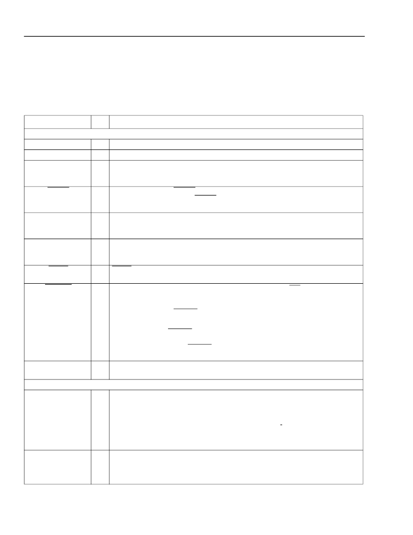
Table 17. Pin Descriptions
Symbol
I/O
Description
Dedicated Pins
V
DD
GND
I/O-V
DD
5
—
—
—
Positive power supply.
Ground supply.
5 V tolerant select. (For 2TxxA only.) All V
DD
5 pins must be tied to either the 5 V power
supply if 5 V tolerant I/O buffers are to be used, or to the 3.3 V power supply (V
DD
) if
they are not. For 2CxxA and 2TxxB devices, these pins are user-programmable I/Os.
During configuration, RESET forces the restart of configuration and a pull-up is
enabled. After configuration, RESET can be used as a general FPGA input or as a
direct input, which causes all PLC latches/FFs to be asynchronously set/reset.
In the master and asynchronous peripheral modes, CCLK is an output which strobes
configuration data in. In the slave or synchronous peripheral mode, CCLK is input syn-
chronous with the data on DIN or D[7:0].
DONE is a bidirectional pin with an optional pull-up resistor. As an active-high, open-
drain output, a high-level on this signal indicates that configuration is complete. As an
input, a low level on DONE delays FPGA start-up after configuration*.
PRGM is an active-low input that forces the restart of configuration and resets the
boundary-scan circuitry. This pin always has an active pull-up.
This pin must be held high during device initialization until the
INIT
pin goes high.
RESET
I
CCLK
I
DONE
I/O
PRGM
I
RD_CFG
I
This pin always has an active pullup.
During configuration,
RD_CFG
is an active-low input that activates the TS_ALL function
and 3-states all of the I/O.
After configuration,
RD_CFG
can be selected (via a bit stream option) to activate the
TS_ALL function as described above, or, if readback is enabled via a bit stream option,
a high-to-low transition on
RD_CFG
will initiate readback of the configuration data,
including PFU output states, starting with frame address 0.
RD_DATA/TDO is a dual-function pin. If used for readback, RD_DATA provides configu-
ration data out. If used in boundary scan, TDO is test data out.
Special-Purpose Pins (Become User I/O After Configuration)
RDY/RCLK
O
During configuration in peripheral mode, RDY indicates another byte can be written to
the FPGA. If a read operation is done when the device is selected, the same status is
also available on D7 in asynchronous peripheral mode. After configuration, the pin is a
user-programmable I/O*.
During the master parallel configuration mode RCLK, which is a read output signal to an
external memory. This output is not normally used. After configuration, this pin is a user-
programmable I/O pin*.
DIN
I
During slave serial or master serial configuration modes, DIN accepts serial configura-
tion data synchronous with CCLK. During parallel configuration modes, DIN is the D0
input. During configuration, a pull-up is enabled, and after configuration, this pin is a
user-programmable I/O pin*.
RD_DATA/TDO
O
* The FPGA States of Operation section contains more information on how to control these signals during start-up. The timing of DONE
release is controlled by one set of bit stream options, and the timing of the simultaneous release of all other configuration pns (and the acti-
vation of all user I/Os) is controlled by a second set of options.
相關(guān)PDF資料 |
PDF描述 |
|---|---|
| OR2T04A-4BA100 | Field-Programmable Gate Arrays |
| OR2T04A-4BA100I | Field-Programmable Gate Arrays |
| OR2T04A-4BA144 | Field-Programmable Gate Arrays |
| OR2T04A-4J160I | Field-Programmable Gate Arrays |
| OR2T04A-4M100 | Field-Programmable Gate Arrays |
相關(guān)代理商/技術(shù)參數(shù) |
參數(shù)描述 |
|---|---|
| OR2T04A-3T208 | 制造商:未知廠家 制造商全稱:未知廠家 功能描述:Field-Programmable Gate Arrays |
| OR2T04A-3T208I | 制造商:未知廠家 制造商全稱:未知廠家 功能描述:Field-Programmable Gate Arrays |
| OR2T04A-3T84 | 制造商:未知廠家 制造商全稱:未知廠家 功能描述:Field-Programmable Gate Arrays |
| OR2T04A-3T84I | 制造商:未知廠家 制造商全稱:未知廠家 功能描述:Field-Programmable Gate Arrays |
| OR2T04A-4BA100 | 制造商:未知廠家 制造商全稱:未知廠家 功能描述:Field-Programmable Gate Arrays |
發(fā)布緊急采購,3分鐘左右您將得到回復(fù)。