- 您現(xiàn)在的位置:買賣IC網(wǎng) > PDF目錄383714 > OR2T04A-3S84I (Electronic Theatre Controls, Inc.) Field-Programmable Gate Arrays PDF資料下載
參數(shù)資料
| 型號: | OR2T04A-3S84I |
| 廠商: | Electronic Theatre Controls, Inc. |
| 元件分類: | FPGA |
| 英文描述: | Field-Programmable Gate Arrays |
| 中文描述: | 現(xiàn)場可編程門陣列 |
| 文件頁數(shù): | 51/192頁 |
| 文件大?。?/td> | 3148K |
| 代理商: | OR2T04A-3S84I |
第1頁第2頁第3頁第4頁第5頁第6頁第7頁第8頁第9頁第10頁第11頁第12頁第13頁第14頁第15頁第16頁第17頁第18頁第19頁第20頁第21頁第22頁第23頁第24頁第25頁第26頁第27頁第28頁第29頁第30頁第31頁第32頁第33頁第34頁第35頁第36頁第37頁第38頁第39頁第40頁第41頁第42頁第43頁第44頁第45頁第46頁第47頁第48頁第49頁第50頁當(dāng)前第51頁第52頁第53頁第54頁第55頁第56頁第57頁第58頁第59頁第60頁第61頁第62頁第63頁第64頁第65頁第66頁第67頁第68頁第69頁第70頁第71頁第72頁第73頁第74頁第75頁第76頁第77頁第78頁第79頁第80頁第81頁第82頁第83頁第84頁第85頁第86頁第87頁第88頁第89頁第90頁第91頁第92頁第93頁第94頁第95頁第96頁第97頁第98頁第99頁第100頁第101頁第102頁第103頁第104頁第105頁第106頁第107頁第108頁第109頁第110頁第111頁第112頁第113頁第114頁第115頁第116頁第117頁第118頁第119頁第120頁第121頁第122頁第123頁第124頁第125頁第126頁第127頁第128頁第129頁第130頁第131頁第132頁第133頁第134頁第135頁第136頁第137頁第138頁第139頁第140頁第141頁第142頁第143頁第144頁第145頁第146頁第147頁第148頁第149頁第150頁第151頁第152頁第153頁第154頁第155頁第156頁第157頁第158頁第159頁第160頁第161頁第162頁第163頁第164頁第165頁第166頁第167頁第168頁第169頁第170頁第171頁第172頁第173頁第174頁第175頁第176頁第177頁第178頁第179頁第180頁第181頁第182頁第183頁第184頁第185頁第186頁第187頁第188頁第189頁第190頁第191頁第192頁
Data Sheet
June 1999
ORCA Series 2 FPGAs
Lucent Technologies Inc.
51
FPGA Configuration Modes
(continued)
Daisy Chain
Multiple FPGAs can be configured by using a daisy
chain of the FPGAs. Daisy chaining uses a lead FPGA
and one or more FPGAs configured in slave serial
mode. The lead FPGA can be configured in any mode
except slave parallel mode. (Daisy chaining is not avail-
able with the boundary-scan ram_w instruction, dis-
cussed later.)
All daisy-chained FPGAs are connected in series.
Each FPGA reads and shifts the preamble and length
count in on positive CCLK and out on negative CCLK
edges.
An upstream FPGA that has received the preamble
and length count outputs a high on DOUT until it has
received the appropriate number of data frames so that
downstream FPGAs do not receive frame start bits
(0s). After loading and retransmitting the preamble and
length count to a daisy chain of slave devices, the lead
device loads its configuration data frames. The loading
of configuration data continues after the lead device
has received its configuration data if its internal frame
bit counter has not reached the length count. When the
configuration RAM is full and the number of bits
received is less than the length count field, the FPGA
shifts any additional data out on DOUT.
The configuration data is read into DIN of slave devices
on the positive edge of CCLK, and shifted out DOUT
on the negative edge of CCLK. Figure 46 shows the
connections for loading multiple FPGAs in a daisy-
chain configuration.
The generation of CCLK for the daisy-chained devices
which are in slave serial mode differs depending on the
configuration mode of the lead device. A master paral-
lel mode device uses its internal timing generator to
produce an internal CCLK at eight times its memory
address rate (RCLK). The asynchronous peripheral
mode device outputs eight CCLKs for each write cycle.
If the lead device is configured in either synchronous
peripheral or a slave mode, CCLK is routed to the lead
device and to all of the daisy-chained devices.
The development system can create a composite
configuration bit stream for configuring daisy-chained
FPGAs. The frame format is a preamble, a length count
for the total bit stream, multiple concatenated data
frames, an end-of-configuration frame per device, a
postamble, and an additional fill bit per device in the
serial chain.
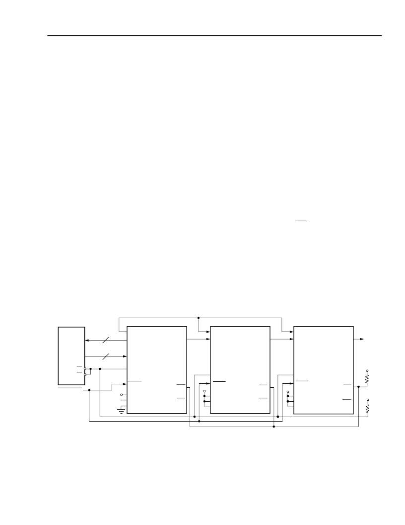
As seen in Figure 46, the
INIT
pins for all of the FPGAs
are connected together. This is required to guarantee
that powerup and initialization will work correctly. In
general, the DONE pins for all of the FPGAs are also
connected together as shown to guarantee that all of
the FPGAs enter the start-up state simultaneously. This
may not be required, depending upon the start-up
sequence desired.
5-4488(F)
Figure 46. Daisy-Chain Configuration Schematic
V
DD
EPROM
PROGRAM
D[7:0]
OE
CE
A[17:0]
A[17:0]
D[7:0]
DONE
M2
M1
M0
DONE
HDC
LDC
RCLK
CCLK
DIN
DOUT
DOUT
DIN
CCLK
DONE
DOUT
INIT
INIT
INIT
CCLK
V
V
DD
OR
GND
PRGM
PRGM
M2
M1
M0
PRGM
M2
M1
M0
V
DD
V
DD
HDC
LDC
RCLK
HDC
LDC
RCLK
V
DD
ORCA
SERIES
FPGA
SLAVE #2
ORCA
SERIES
FPGA
MASTER
ORCA
SERIES
FPGA
SLAVE #1
相關(guān)PDF資料 |
PDF描述 |
|---|---|
| OR2T04A-4BA208 | Field-Programmable Gate Arrays |
| OR2T04A-4BA208I | Field-Programmable Gate Arrays |
| OR2T04A-4BA84 | Field-Programmable Gate Arrays |
| OR2T04A-4BA84I | Field-Programmable Gate Arrays |
| OR2T04A-4BC100 | Field-Programmable Gate Arrays |
相關(guān)代理商/技術(shù)參數(shù) |
參數(shù)描述 |
|---|---|
| OR2T04A-3T100 | 制造商:未知廠家 制造商全稱:未知廠家 功能描述:Field-Programmable Gate Arrays |
| OR2T04A-3T100I | 制造商:未知廠家 制造商全稱:未知廠家 功能描述:Field-Programmable Gate Arrays |
| OR2T04A-3T144 | 制造商:未知廠家 制造商全稱:未知廠家 功能描述:Field-Programmable Gate Arrays |
| OR2T04A-3T144I | 制造商:未知廠家 制造商全稱:未知廠家 功能描述:Field-Programmable Gate Arrays |
| OR2T04A-3T160 | 制造商:未知廠家 制造商全稱:未知廠家 功能描述:Field-Programmable Gate Arrays |
發(fā)布緊急采購,3分鐘左右您將得到回復(fù)。