- 您現(xiàn)在的位置:買賣IC網(wǎng) > PDF目錄383714 > OR2T04A-3S160 (Electronic Theatre Controls, Inc.) Field-Programmable Gate Arrays PDF資料下載
參數(shù)資料
| 型號(hào): | OR2T04A-3S160 |
| 廠商: | Electronic Theatre Controls, Inc. |
| 元件分類: | FPGA |
| 英文描述: | Field-Programmable Gate Arrays |
| 中文描述: | 現(xiàn)場可編程門陣列 |
| 文件頁數(shù): | 49/192頁 |
| 文件大小: | 3148K |
| 代理商: | OR2T04A-3S160 |
第1頁第2頁第3頁第4頁第5頁第6頁第7頁第8頁第9頁第10頁第11頁第12頁第13頁第14頁第15頁第16頁第17頁第18頁第19頁第20頁第21頁第22頁第23頁第24頁第25頁第26頁第27頁第28頁第29頁第30頁第31頁第32頁第33頁第34頁第35頁第36頁第37頁第38頁第39頁第40頁第41頁第42頁第43頁第44頁第45頁第46頁第47頁第48頁當(dāng)前第49頁第50頁第51頁第52頁第53頁第54頁第55頁第56頁第57頁第58頁第59頁第60頁第61頁第62頁第63頁第64頁第65頁第66頁第67頁第68頁第69頁第70頁第71頁第72頁第73頁第74頁第75頁第76頁第77頁第78頁第79頁第80頁第81頁第82頁第83頁第84頁第85頁第86頁第87頁第88頁第89頁第90頁第91頁第92頁第93頁第94頁第95頁第96頁第97頁第98頁第99頁第100頁第101頁第102頁第103頁第104頁第105頁第106頁第107頁第108頁第109頁第110頁第111頁第112頁第113頁第114頁第115頁第116頁第117頁第118頁第119頁第120頁第121頁第122頁第123頁第124頁第125頁第126頁第127頁第128頁第129頁第130頁第131頁第132頁第133頁第134頁第135頁第136頁第137頁第138頁第139頁第140頁第141頁第142頁第143頁第144頁第145頁第146頁第147頁第148頁第149頁第150頁第151頁第152頁第153頁第154頁第155頁第156頁第157頁第158頁第159頁第160頁第161頁第162頁第163頁第164頁第165頁第166頁第167頁第168頁第169頁第170頁第171頁第172頁第173頁第174頁第175頁第176頁第177頁第178頁第179頁第180頁第181頁第182頁第183頁第184頁第185頁第186頁第187頁第188頁第189頁第190頁第191頁第192頁
Lucent Technologies Inc.
49
Data Sheet
June 1999
ORCA Series 2 FPGAs
FPGA Configuration Modes
(continued)
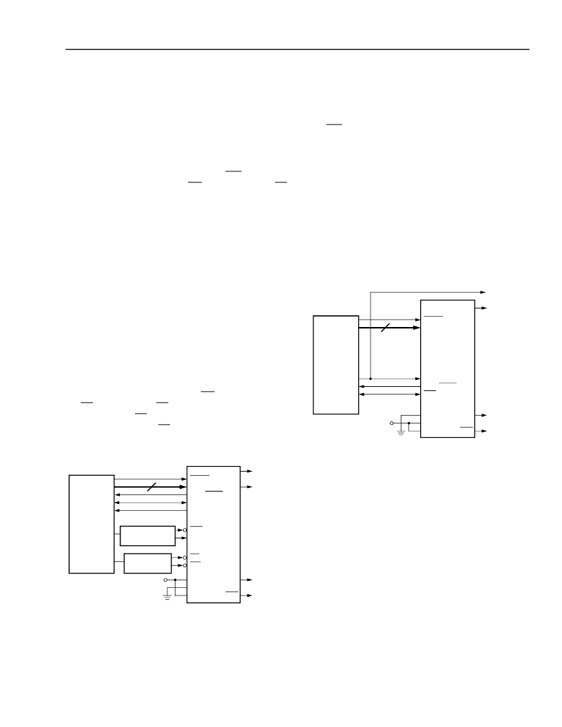
Asynchronous Peripheral Mode
Figure 42 shows the connections needed for the asyn-
chronous peripheral mode. In this mode, the FPGA
system interface is similar to that of a microprocessor-
peripheral interface. The microprocessor generates the
control signals to write an 8-bit byte into the FPGA. The
FPGA control inputs include active-low
CS0
and active-
high CS1 chip selects, a write
WR
input, and a read
RD
input. The chip selects can be cycled or maintained at
a static level during the configuration cycle. Each byte
of data is written into the FPGA’s D[7:0] input pins.
The FPGA provides a RDY status output to indicate
that another byte can be loaded. A low on RDY indi-
cates that the double-buffered hold/shift registers are
not ready to receive data, and this pin must be moni-
tored to go high before another byte of data can be
written. The shortest time RDY is low occurs when a
byte is loaded into the hold register and the shift regis-
ter is empty, in which case the byte is immediately
transferred to the shift register. The longest time for
RDY to remain low occurs when a byte is loaded into
the holding register and the shift register has just
started shifting configuration data into configuration
RAM.
The RDY status is also available on the D7 pin by
enabling the chip selects, setting
WR
high, and apply-
ing
RD
low, where the
RD
input is an output enable for
the D7 pin when
RD
is low. The D[6:0] pins are not
enabled to drive when
RD
is low and, thus, only act as
input pins in asynchronous peripheral mode.
5-4484(F)
Figure 42. Asynchronous Peripheral Configuration
Schematic
Synchronous Peripheral Mode
In the synchronous peripheral mode, byte-wide data is
input into D[7:0] on the rising edge of the CCLK input.
The first data byte is clocked in on the second CCLK
after
INIT
goes high. Subsequent data bytes are
clocked in on every eighth rising edge of CCLK. The
RDY signal is an output which acts as an acknowledge.
RDY goes high one CCLK after data is clocked and,
after one CCLK cycle, returns low. The process repeats
until all of the data is loaded into the FPGA. The data
begins shifting on DOUT 1.5 cycles after it is loaded in
parallel. It requires additional CCLKs after the last byte
is loaded to complete the shifting. Figure 43 shows the
connections for synchronous peripheral mode.
As with master modes, the peripheral modes can be
used as the lead FPGA for a daisy chain of slave
FPGAs.
5-4486(F)
Figure 43. Synchronous Peripheral Configuration
Schematic
TO DAISY-
CHAINED
DEVICES
DOUT
CCLK
HDC
LDC
V
DD
ORCA
SERIES
FPGA
MICRO-
PROCESSOR
ADDRESS
DECODE LOGIC
BUS
CONTROLLER
PRGM
D[7:0]
RDY/BUSY
INIT
DONE
CS0
CS1
RD
WR
M2
M1
M0
8
TO DAISY-
CHAINED
DEVICES
DOUT
HDC
LDC
ORCA
SERIES
FPGA
MICRO-
PROCESSOR
PRGM
D[7:0]
M2
M1
M0
8
+5 V
CCLK
RDY/BUSY
INIT
相關(guān)PDF資料 |
PDF描述 |
|---|---|
| OR2T04A-3S160I | Field-Programmable Gate Arrays |
| OR2T04A-3S208 | Field-Programmable Gate Arrays |
| OR2T04A-3S208I | Ceramic Chip Capacitors / MIL-PRF-55681; Capacitance [nom]: 100pF; Working Voltage (Vdc)[max]: 100V; Capacitance Tolerance: +/-10%; Dielectric: Multilayer Ceramic; Temperature Coefficient: C0G (NP0); Lead Style: Surface Mount Chip; Lead Dimensions: 1206; Termination: Solder Coated SnPb; Body Dimensions: 0.125" x 0.062" x 0.051"; Container: Bag; Features: MIL-PRF-55681: S Failure Rate |
| OR2T04A-3S84 | Field-Programmable Gate Arrays |
| OR2T04A-3S84I | Field-Programmable Gate Arrays |
相關(guān)代理商/技術(shù)參數(shù) |
參數(shù)描述 |
|---|---|
| OR2T04A-3S160I | 制造商:未知廠家 制造商全稱:未知廠家 功能描述:Field-Programmable Gate Arrays |
| OR2T04A-3S208 | 制造商:未知廠家 制造商全稱:未知廠家 功能描述:Field-Programmable Gate Arrays |
| OR2T04A-3S208I | 制造商:未知廠家 制造商全稱:未知廠家 功能描述:Field-Programmable Gate Arrays |
| OR2T04A-3S84 | 制造商:未知廠家 制造商全稱:未知廠家 功能描述:Field-Programmable Gate Arrays |
| OR2T04A-3S84I | 制造商:未知廠家 制造商全稱:未知廠家 功能描述:Field-Programmable Gate Arrays |
發(fā)布緊急采購,3分鐘左右您將得到回復(fù)。