- 您現(xiàn)在的位置:買賣IC網(wǎng) > PDF目錄383706 > OR2T04A-3J84I (Electronic Theatre Controls, Inc.) Field-Programmable Gate Arrays PDF資料下載
參數(shù)資料
| 型號: | OR2T04A-3J84I |
| 廠商: | Electronic Theatre Controls, Inc. |
| 元件分類: | FPGA |
| 英文描述: | Field-Programmable Gate Arrays |
| 中文描述: | 現(xiàn)場可編程門陣列 |
| 文件頁數(shù): | 6/192頁 |
| 文件大小: | 3148K |
| 代理商: | OR2T04A-3J84I |
第1頁第2頁第3頁第4頁第5頁當前第6頁第7頁第8頁第9頁第10頁第11頁第12頁第13頁第14頁第15頁第16頁第17頁第18頁第19頁第20頁第21頁第22頁第23頁第24頁第25頁第26頁第27頁第28頁第29頁第30頁第31頁第32頁第33頁第34頁第35頁第36頁第37頁第38頁第39頁第40頁第41頁第42頁第43頁第44頁第45頁第46頁第47頁第48頁第49頁第50頁第51頁第52頁第53頁第54頁第55頁第56頁第57頁第58頁第59頁第60頁第61頁第62頁第63頁第64頁第65頁第66頁第67頁第68頁第69頁第70頁第71頁第72頁第73頁第74頁第75頁第76頁第77頁第78頁第79頁第80頁第81頁第82頁第83頁第84頁第85頁第86頁第87頁第88頁第89頁第90頁第91頁第92頁第93頁第94頁第95頁第96頁第97頁第98頁第99頁第100頁第101頁第102頁第103頁第104頁第105頁第106頁第107頁第108頁第109頁第110頁第111頁第112頁第113頁第114頁第115頁第116頁第117頁第118頁第119頁第120頁第121頁第122頁第123頁第124頁第125頁第126頁第127頁第128頁第129頁第130頁第131頁第132頁第133頁第134頁第135頁第136頁第137頁第138頁第139頁第140頁第141頁第142頁第143頁第144頁第145頁第146頁第147頁第148頁第149頁第150頁第151頁第152頁第153頁第154頁第155頁第156頁第157頁第158頁第159頁第160頁第161頁第162頁第163頁第164頁第165頁第166頁第167頁第168頁第169頁第170頁第171頁第172頁第173頁第174頁第175頁第176頁第177頁第178頁第179頁第180頁第181頁第182頁第183頁第184頁第185頁第186頁第187頁第188頁第189頁第190頁第191頁第192頁
Data Sheet
June 1999
ORCA Series 2 FPGAs
6
Lucent Technologies Inc.
Programmable Logic Cells
(continued))
Key: C = controlled by configuration RAM.
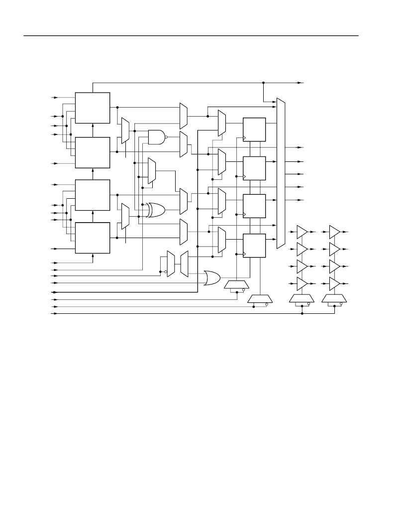
Figure 3. Simplified PFU Diagram
5-4573(F)
A4
A3
A2
A1
A4
A3
A2
A1
QLUT3
A0
CARRY
CARRY
A3
A2
A1
A0
QLUT2
B4
B3
B2
B1
B4
B3
B2
B1
QLUT1
B0
CARRY
CARRY
B3
B2
B1
B0
QLUT0
CIN
C0
LSR
GSR
WD[3:0]
CK
CKEN
TRI
PFU_XOR
B4
A4
PFU_NAND
PFU_MUX
C
C
C
C
WD3
WD2
WD1
WD0
C
C
C
T
T
T
T
REG3
SR
EN
REG2
SR
EN
REG1
SR
EN
REG0
SR
EN
O4
O3
O2
O1
O0
F3
C
C
COUT
F2
F1
F0
D0
D1
D2
D3
Q0
Q1
Q2
Q3
C
T
T
T
T
C
Figure 2 and Figure 3 show high-level and detailed
views of the ports in the PFU, respectively. The ports
are referenced with a two- to four-character suffix to a
PFU’s location. As mentioned, there are two 5-bit input
data buses (A[4:0] and B[4:0]) to the LUT, one 4-bit
input data bus (WD[3:0]) to the latches/FFs, and an
output data bus (O[4:0]).
Figure 3 shows the four latches/FFs (REG[3:0]) and the
64-bit look-up table (QLUT[3:0]) in the PFU. The PFU
does combinatorial logic in the LUT and sequential
logic in the latches/FFs. The LUT is static random
access memory (SRAM) and can be used for read/
write or read-only memory. The eight 3-state buffers
found in each PLC are also shown, although they actu-
ally reside external to the PFU.
Each latch/FF can accept data from the LUT. Alterna-
tively, the latches/FFs can accept direct data from
WD[3:0], eliminating the LUT delay if no combinatorial
function is needed. The LUT outputs can bypass the
latches/FFs, which reduces the delay out of the PFU. It
is possible to use the LUT and latches/FFs more or
less independently. For example, the latches/FFs can
be used as a 4-bit shift register, and the LUT can be
used to detect when a register has a particular pattern
in it.
相關PDF資料 |
PDF描述 |
|---|---|
| OR2T04A-3PS144 | Field-Programmable Gate Arrays |
| OR2T04A-3PS144I | Field-Programmable Gate Arrays |
| OR2T04A-3PS160 | Field-Programmable Gate Arrays |
| OR2T04A-3PS160I | Field-Programmable Gate Arrays |
| OR2C40A-3S304 | Field-Programmable Gate Arrays |
相關代理商/技術參數(shù) |
參數(shù)描述 |
|---|---|
| OR2T04A-3M100 | 制造商:未知廠家 制造商全稱:未知廠家 功能描述:Field-Programmable Gate Arrays |
| OR2T04A-3M100I | 制造商:未知廠家 制造商全稱:未知廠家 功能描述:Field-Programmable Gate Arrays |
| OR2T04A-3M144 | 制造商:未知廠家 制造商全稱:未知廠家 功能描述:Field-Programmable Gate Arrays |
| OR2T04A-3M144I | 制造商:未知廠家 制造商全稱:未知廠家 功能描述:Field-Programmable Gate Arrays |
| OR2T04A-3M160 | 制造商:未知廠家 制造商全稱:未知廠家 功能描述:Field-Programmable Gate Arrays |
發(fā)布緊急采購,3分鐘左右您將得到回復。