- 您現(xiàn)在的位置:買賣IC網(wǎng) > PDF目錄383708 > OR2T04A-2BC84 (Electronic Theatre Controls, Inc.) Field-Programmable Gate Arrays PDF資料下載
參數(shù)資料
| 型號: | OR2T04A-2BC84 |
| 廠商: | Electronic Theatre Controls, Inc. |
| 元件分類: | FPGA |
| 英文描述: | Field-Programmable Gate Arrays |
| 中文描述: | 現(xiàn)場可編程門陣列 |
| 文件頁數(shù): | 68/192頁 |
| 文件大?。?/td> | 3148K |
| 代理商: | OR2T04A-2BC84 |
第1頁第2頁第3頁第4頁第5頁第6頁第7頁第8頁第9頁第10頁第11頁第12頁第13頁第14頁第15頁第16頁第17頁第18頁第19頁第20頁第21頁第22頁第23頁第24頁第25頁第26頁第27頁第28頁第29頁第30頁第31頁第32頁第33頁第34頁第35頁第36頁第37頁第38頁第39頁第40頁第41頁第42頁第43頁第44頁第45頁第46頁第47頁第48頁第49頁第50頁第51頁第52頁第53頁第54頁第55頁第56頁第57頁第58頁第59頁第60頁第61頁第62頁第63頁第64頁第65頁第66頁第67頁當(dāng)前第68頁第69頁第70頁第71頁第72頁第73頁第74頁第75頁第76頁第77頁第78頁第79頁第80頁第81頁第82頁第83頁第84頁第85頁第86頁第87頁第88頁第89頁第90頁第91頁第92頁第93頁第94頁第95頁第96頁第97頁第98頁第99頁第100頁第101頁第102頁第103頁第104頁第105頁第106頁第107頁第108頁第109頁第110頁第111頁第112頁第113頁第114頁第115頁第116頁第117頁第118頁第119頁第120頁第121頁第122頁第123頁第124頁第125頁第126頁第127頁第128頁第129頁第130頁第131頁第132頁第133頁第134頁第135頁第136頁第137頁第138頁第139頁第140頁第141頁第142頁第143頁第144頁第145頁第146頁第147頁第148頁第149頁第150頁第151頁第152頁第153頁第154頁第155頁第156頁第157頁第158頁第159頁第160頁第161頁第162頁第163頁第164頁第165頁第166頁第167頁第168頁第169頁第170頁第171頁第172頁第173頁第174頁第175頁第176頁第177頁第178頁第179頁第180頁第181頁第182頁第183頁第184頁第185頁第186頁第187頁第188頁第189頁第190頁第191頁第192頁
Data Sheet
June 1999
ORCA Series 2 FPGAs
68
Lucent Technologies Inc.
Pin Information
(continued)
Package Compatibility
The package pinouts are consistent across ORCA
Series FPGAs with the following exception:
some
user
I/O pins that do not have any special functions will
be converted to V
DD
5 pins for the OR2TxxA series
.
If the designer does not use these pins for the
OR2CxxA and OR2TxxB series, then pinout compati-
bility will be maintained between the ORCA OR2CxxA,
OR2TxxA, and OR2TxxB series of FPGAs. Note that
they must be connected to a power supply for the
OR2TxxA series.
Package pinouts being consistent across all ORCA
Series FPGAs enables a designer to select a package
based on I/O requirements and change the FPGA with-
out laying out the printed-circuit board again. The
change might be to a larger FPGA if additional func-
tionality is needed, or it might be to a smaller FPGA to
decrease unit cost.
Table 18A provides the number of user I/Os available
for the ORCA OR2CxxA and OR2TxxB Series FPGAs
for each available package, and Table 18B provides the
number of user I/Os available in the ORCAOR2TxxA
series. It should be noted that the number of user I/Os
available for the OR2TxxA series is reduced from the
equivalent OR2CxxA devices by the number of
required V
DD
5 pins, as shown in Table 18B. The pins
that are converted from user I/O to V
DD
5 are denoted
as I/O-V
DD
5 in the pin information tables (Table 19
through 28). Each package has six dedicated configu-
ration pins.
Table 19—Table 28. provide the package pin and pin
function for the ORCA Series 2 FPGAs and packages.
The bond pad name is identified in the PIC nomencla-
ture used in the ORCA Foundry design editor.
When the number of FPGA bond pads exceeds the
number of package pins, bond pads are unused. When
the number of package pins exceeds the number of
bond pads, package pins are left unconnected (no
connects). When a package pin is to be left as a no
connect for a specific die, it is indicated as a note in the
device pad column for the FPGA. The tables provide no
information on unused pads.
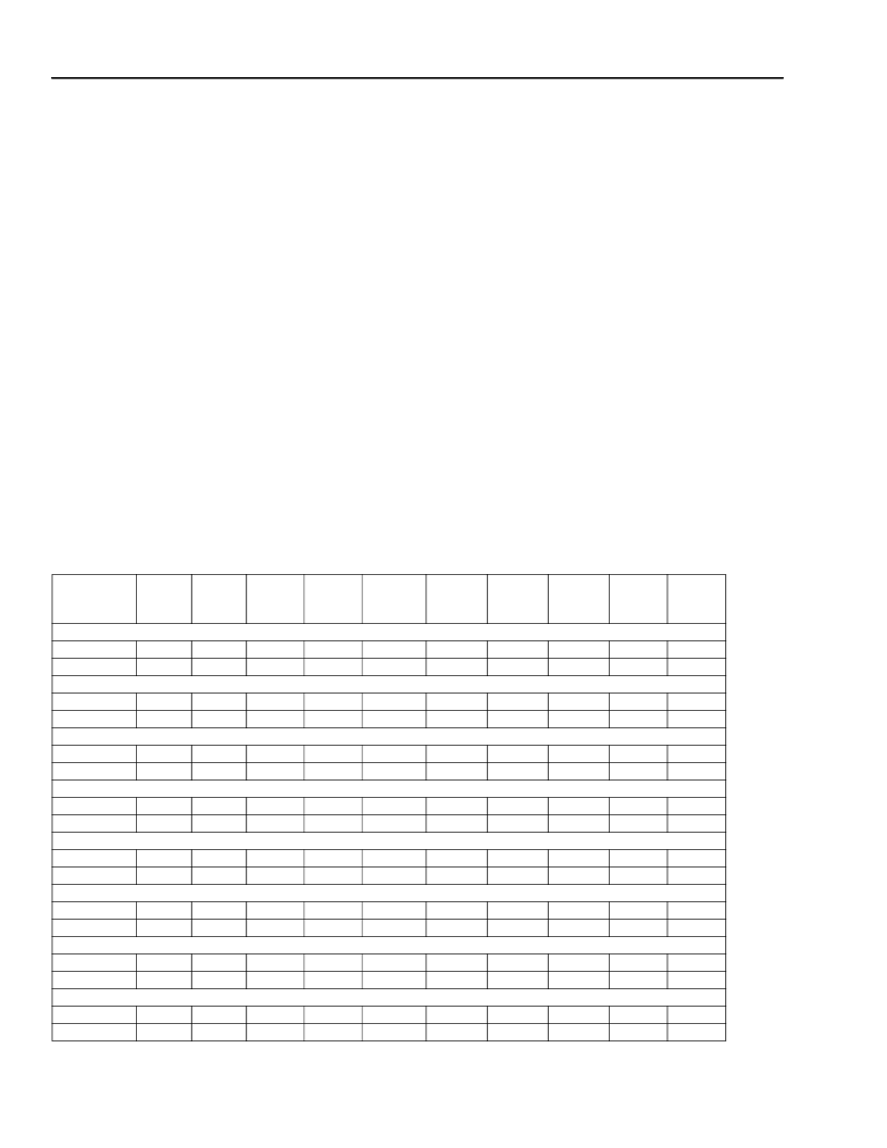
Table 18A. ORCAOR2CxxA and OR2TxxB Series FPGA I/Os Summary
* 432 EBGA not available for OR2T15B
Device
84-Pin
PLCC
100-Pin
TQFP
144-Pin
TQFP
160-Pin
QFP
208-Pin
SQFP/
SQFP2
240-Pin
SQFP/
SQFP2
256-Pin
PBGA
304-Pin
SQFP/
SQFP2
352-Pin
PBGA
432-Pin
EBGA
OR2C04A
User I/Os
V
DD
/V
SS
OR2C06A
User I/Os
V
DD
/V
SS
OR2C08A
User I/Os
V
DD
/V
SS
OR2C10A
User I/Os
V
DD
/V
SS
OR2C12A
User I/Os
V
DD
/V
SS
OR2C15A/OR2T15B
User I/Os
V
DD
/V
SS
OR2C26A
User I/Os
V
DD
/V
SS
OR2C40A/OR2T40B
User I/Os
V
DD
/V
SS
64
14
77
17
114
24
130
24
160
31
—
—
—
—
—
—
—
—
—
—
64
14
77
17
114
24
130
24
171
31
192
42
192
26
—
—
—
—
—
—
64
14
—
—
—
—
130
24
171
31
192
40
221
26
—
—
—
—
—
—
64
14
—
—
—
—
130
24
171
31
192
40
221
26
—
—
256
48
—
—
64
14
—
—
—
—
—
—
171
31
192
42
223
26
252
46
288
48
—
—
64
14
—
—
—
—
—
—
171
31
192
42
223
26
252
46
298
48
320*
84
—
—
—
—
—
—
—
—
171
31
192
42
—
—
252
46
298
48
342
84
—
—
—
—
—
—
—
—
171
31
192
42
—
—
252
46
—
—
342
84
相關(guān)PDF資料 |
PDF描述 |
|---|---|
| OR2T04A-4BA144I | Field-Programmable Gate Arrays |
| OR2T04A-4BA160 | Field-Programmable Gate Arrays |
| OR2T04A-2T160I | Field-Programmable Gate Arrays |
| OR2T04A-3BA100 | Field-Programmable Gate Arrays |
| OR2T04A-3BA100I | Field-Programmable Gate Arrays |
相關(guān)代理商/技術(shù)參數(shù) |
參數(shù)描述 |
|---|---|
| OR2T04A-2BC84I | 制造商:未知廠家 制造商全稱:未知廠家 功能描述:Field-Programmable Gate Arrays |
| OR2T04A-2J100 | 制造商:未知廠家 制造商全稱:未知廠家 功能描述:Field-Programmable Gate Arrays |
| OR2T04A-2J100I | 制造商:未知廠家 制造商全稱:未知廠家 功能描述:Field-Programmable Gate Arrays |
| OR2T04A-2J144 | 制造商:未知廠家 制造商全稱:未知廠家 功能描述:Field-Programmable Gate Arrays |
| OR2T04A-2J144I | 制造商:未知廠家 制造商全稱:未知廠家 功能描述:Field-Programmable Gate Arrays |
發(fā)布緊急采購,3分鐘左右您將得到回復(fù)。