- 您現(xiàn)在的位置:買賣IC網(wǎng) > PDF目錄383693 > OPA622AP OP-AMP|SINGLE|BIPOLAR|DIP|14PIN|PLASTIC PDF資料下載
參數(shù)資料
| 型號: | OPA622AP |
| 英文描述: | OP-AMP|SINGLE|BIPOLAR|DIP|14PIN|PLASTIC |
| 中文描述: | 運放|單|雙極|雙酯| 14PIN |塑料 |
| 文件頁數(shù): | 4/18頁 |
| 文件大小: | 335K |
| 代理商: | OPA622AP |
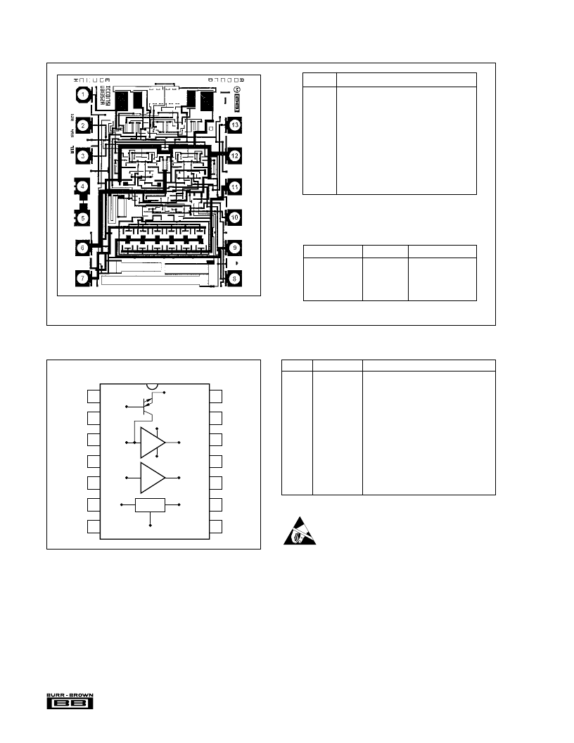
OPA622
4
PAD
FUNCTION
1
2
3
4
5
6
7
8
9
10
11
12
13
Quiescent Current Adjustment
Inverting Analog Input
Non-Inverting Analog Input
NC
NC
–5V Supply
–5V Supply, Output
Inverting Buffer Output
Analog Output
Analog OTA Output
+5V Supply, Output
+5V Supply
Non-Inverting Buffer Output
Substrate Bias:
Negative Supply
NC:
No Connection
Wire Bonding: Gold wire bonding is recommended.
DICE INFORMATION
MECHANICAL INFORMATION
MILS (0.001")
MILLIMETERS
Die Size
Die Thickness
Min. Pad Size
Backing: Titanium
Gold
57 x 69
±
5
14
±
1
4 x 4
0.02+0.05,–0.0
0.30
±
0.05
1.44 x 1.76
±
0.13
0.55
±
0.025
0.10 x 0.10
0.0005+0.0013, –0.0
0.0076
±
0.0013
OPA622AD DIE TOPOGRAPHY
PIN NO.
DESCRIPTION
FUNCTION
1
2
3
4
5
6
NC
No Connection
Quiescent Current Adjustment; typical 3-8mA
Inverting Analog Input
Noninverting Analog Input
Negative Supply Voltage; typical –5VDC
Negative Supply Voltage Output Buffer;
typical –5VDC
Analog Output Feedback Buffer
Analog Output
Analog Output OTA
Positive Supply Voltage Output Buffer; typical
+5VDC
Positive Supply Voltage; typical +5VDC
Analog Output/Input
No Connection
I
Q
Adjust
–In
+In
–V
CC
–V
CC OUT
8
9
BUF–
V
OTA
+V
CC OUT
10
11
12
13
14
+V
BUF+
NC
PIN CONFIGURATION
FUNCTIONAL DESCRIPTION
NC
I
Q
Adjust
–In
+In
–V
CC
–V
CC OUT
NC
NC
BUF+
+V
CC
+V
CC OUT
OTA
V
OUT
BUF–
1
2
3
4
5
6
7
OPA622
14
13
12
11
10
9
8
FB
OTA
OB
13
4
10
3
5
12
2
Biasing
11
6
8
SO/DIP
9
Top View
ELECTROSTATIC
DISCHARGE SENSITIVITY
Electrostatic discharge can cause damage ranging from per-
formance degradation to complete device failure. Burr-
Brown Corporation recommends that all integrated circuits
be handled and stored using appropriate ESD protection
methods.
ESD damage can range from subtle performance degrada-
tion to complete device failure. Precision integrated circuits
may be more susceptible to damage because very small
parametric changes could cause the device not to meet
published specifications.
相關PDF資料 |
PDF描述 |
|---|---|
| OPA622AU | OP-AMP|SINGLE|BIPOLAR|SOP|14PIN|PLASTIC |
| OPA623 | Wide Bandwidth, Current-Feedback OPERATIONAL AMPLIFIER |
| OPA623AP | Wide Bandwidth, Current-Feedback OPERATIONAL AMPLIFIER |
| OPA623AU | Wide Bandwidth, Current-Feedback OPERATIONAL AMPLIFIER |
| OPA628AU | Low Distortion Wideband OPERATIONAL AMPLIFIER |
相關代理商/技術參數(shù) |
參數(shù)描述 |
|---|---|
| OPA622AU | 制造商:BB 制造商全稱:BB 功能描述:Wide-Bandwidth OPERATIONAL AMPLIFIER |
| OPA623 | 制造商:BB 制造商全稱:BB 功能描述:Wide Bandwidth, Current-Feedback OPERATIONAL AMPLIFIER |
| OPA623 WAF | 制造商:Texas Instruments 功能描述: |
| OPA623AP | 制造商:BB 制造商全稱:BB 功能描述:Wide Bandwidth, Current-Feedback OPERATIONAL AMPLIFIER |
| OPA623AU | 制造商:BB 制造商全稱:BB 功能描述:Wide Bandwidth, Current-Feedback OPERATIONAL AMPLIFIER |
發(fā)布緊急采購,3分鐘左右您將得到回復。