- 您現(xiàn)在的位置:買(mǎi)賣(mài)IC網(wǎng) > PDF目錄382364 > NWK914GP1N (Mitel Networks Corporation) PHY/PMD High Speed Copper Media Transceiver PDF資料下載
參數(shù)資料
| 型號(hào): | NWK914GP1N |
| 廠(chǎng)商: | Mitel Networks Corporation |
| 英文描述: | PHY/PMD High Speed Copper Media Transceiver |
| 中文描述: | 物理層/ PMD的高速銅媒體收發(fā)器 |
| 文件頁(yè)數(shù): | 3/9頁(yè) |
| 文件大?。?/td> | 122K |
| 代理商: | NWK914GP1N |

3
NWK914D
NRZ to MLT3 Encoder
The serial data from the shifter then passes through an
encoder which converts the NRZI binary data into the three
level MLT-3 format for transmission by the 'TXO' outputs.
Transmit Line Drivers
There are two on-chip Line Drivers both of which share
the output pins TXOP and TXON. The N10/100 pin is used
to control which driver is active and allowed to drive the line.
When held high the MLT-3 data is output by the 100Mb/s
driver. This driver consists of differential current source
outputs with programmable sink capability, designed to
drive a nominal output impedance of 50
.
Output current is set by the value of an external resistor
(R
REF
) between pin 'TXREF' and 'TXGND'.
This resistor defines an internal reference current derived
from an on-chip bandgap reference.
Final output current at the 'TXO' outputs is a multiple of
this current and is defined as:-
I
TXO
(mA) = 52/R
REF
(k
)
Transition times of the 'TXO' outputs are matched and
internally limited to approx. 2.5ns to reduce EMI emissions.
FUNCTIONAL DESCRIPTION
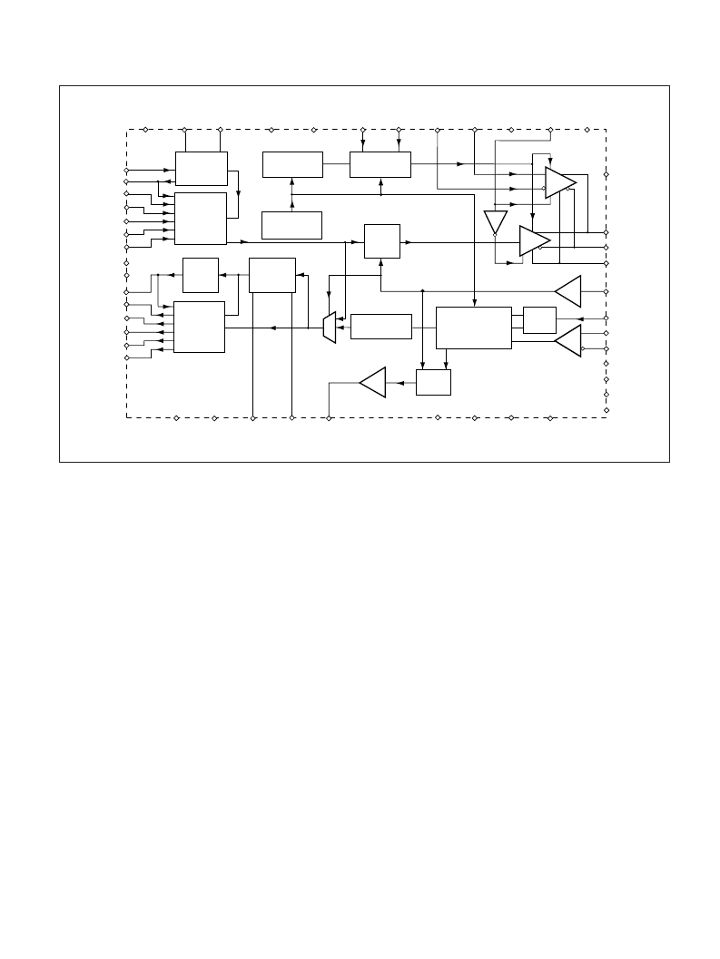
The functional blocks within the device are shown in Fig. 3.
These are described below:-
Transmit Section
Times Five Clock Multiplier 25MHz to 125MHz
This circuit consists of a phase lock loop (PLL) that is
operating at 125MHz, centre frequency. The 125MHz is
divided by 5 to produce a 25MHz clock which is phase
compared with a 25MHz crystal clock reference frequency
which is input on pin REFCLK. The 25MHz clock (pin TXC)
is then sent to the PCS layer to clock in in the 5 bit nibble
data. Pins LFTA and LFTB are provided to set the VCO
characteristics. The recommended loop filter components
are shown in Fig.6.
A control current is derived from the clock multiplier and
is used by the receive clock recovery circuit to centre the
PLL when no input data is present.
Five Bit Nibble to 125MHz Shifter
Data is input to the transmit side in 5 bit wide parallel
form on pins TDAT0 through TDAT4. This NRZ data is
clocked in on the positive edge of the 25MHz clock pin TXC.
The parallel data is first loaded into a 5 bit wide register prior
to being loaded into a 5 bit PISO where it is converted into
a serial data stream. The last stage of the shifter incorporates
a converter to change the data from NRZ to NRZI.
Fig.3 System block diagram
LBEN
TTLGND1
TXREF
REFCLK
LOW VOLTAGE
SHUT DOWN
EQSEL
RXIP
RXIN
SUBGND
TXOP
TXON
3
LEVEL
TXGND
RXV
CC
1
RXGND
RXV
CC
2
TXPLLV
CC
125
MHz
TDLV
CC
RXPLLV
CC
TIMES FIVE
CLOCK
MULTIPLIER
SIGNAL
DETECT
ADAPTIVE
EQUALIZER
MLT-3 to NRZI
COMPARATORS
NRZI
to
MLT-3
DIVIDE
CLOCK
by FIVE
RDAT0
RDAT1
RDAT2
RDAT3
RDAT4
RXC
TDAT0
TDAT1
TDAT2
TDAT3
TDAT4
TXC
LFTB
TEST
N10/100
10T
X
IN
10T
X
IP
CURRENT
REFERENCE
LFRA
NRZ to NRZI
SHIFTER &
NRZI to NRZ
SDT
BGAPV
CC
BGAPGND
RDLV
CC
LFTA
TTLV
CC
TXV
CC
TTLGND2
LFRB
CLOCK
RECOVERY
PLL,125MHZ
TTL
TESTIP
TXPLLGND
RXPLLGND
BAND GAP
VOLTAGE
REFERENCE
SHIFTER &
100
10
Mb/s
TTL
TXOE
相關(guān)PDF資料 |
PDF描述 |
|---|---|
| NWK933 | 3.3V 10/100 Fast Ethernet Transceiver to MII |
| NWK933CG | 3.3V 10/100 Fast Ethernet Transceiver to MII |
| NWK933TP1N | MUSHROOM CAP-YLW OP RoHS Compliant: Yes |
| NWK954 | QUAD FAST ETHERNET REPEATER |
| NWK954CG | QUAD FAST ETHERNET REPEATER |
相關(guān)代理商/技術(shù)參數(shù) |
參數(shù)描述 |
|---|---|
| NWK914S | 制造商:ZARLINK 制造商全稱(chēng):Zarlink Semiconductor Inc 功能描述:PHY/PMD High Speed Copper Media Transceiver |
| NWK914SCGGH1N | 制造商:未知廠(chǎng)家 制造商全稱(chēng):未知廠(chǎng)家 功能描述:LAN Transceiver |
| NWK918CGGH1N | 制造商:未知廠(chǎng)家 制造商全稱(chēng):未知廠(chǎng)家 功能描述:LAN Transceiver |
| NWK933 | 制造商:MITEL 制造商全稱(chēng):Mitel Networks Corporation 功能描述:3.3V 10/100 Fast Ethernet Transceiver to MII |
| NWK933CG | 制造商:MITEL 制造商全稱(chēng):Mitel Networks Corporation 功能描述:3.3V 10/100 Fast Ethernet Transceiver to MII |
發(fā)布緊急采購(gòu),3分鐘左右您將得到回復(fù)。