- 您現(xiàn)在的位置:買賣IC網(wǎng) > PDF目錄361112 > NE5517NG (ON SEMICONDUCTOR) Dual Operational Transconductance Amplifier PDF資料下載
參數(shù)資料
| 型號: | NE5517NG |
| 廠商: | ON SEMICONDUCTOR |
| 元件分類: | 運(yùn)算放大器 |
| 英文描述: | Dual Operational Transconductance Amplifier |
| 中文描述: | DUAL OP-AMP, 5000 uV OFFSET-MAX, 2 MHz BAND WIDTH, PDIP16 |
| 封裝: | LEAD FREE, PLASTIC, DIP-16 |
| 文件頁數(shù): | 8/14頁 |
| 文件大小: | 194K |
| 代理商: | NE5517NG |
NE5517, NE5517A, AU5517
http://onsemi.com
8
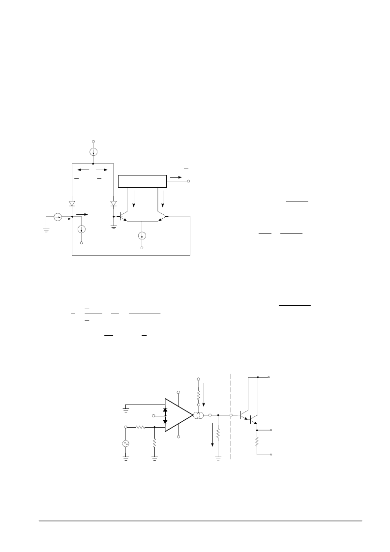
Linearizing Diodes
For V
IN
greater than a few millivolts, Equation 3 becomes
invalid and the transconductance increases non-linearly.
Figure 22 shows how the internal diodes can linearize the
transfer function of the operational amplifier. Assume D
2
and D
3
are biased with current sources and the input signal
current is I
S
. Since I
4
+ I
5
= I
B
and I
5
I
4
= I
0
,
that is: I
4
= (I
B
I
0
), I
5
= (I
B
+ I
0
)
+VS
I
D
I
B
I
5
Q
4
1/2I
D
I
S
I
S
1/2I
D
VS
I
4
I
5
D
3
D
2
ID
2
IS
ID
2
IS
I0
I5
I4
I0
2 IS
IB
ID
Figure 22. Linearizing Diode
For the diodes and the input transistors that have identical
geometries and are subject to similar voltages and
temperatures, the following equation is true:
T
ID
2
ID
2
I
S
I
S
KT
q
In1 2(I
B
1 2(I
B
I
O
)
I
O
)
(eq. 6)
I
O
I
S
2
I
B
I
D
for |I
S
|
I
D
2
The only limitation is that the signal current should not
exceed I
D
.
Impedance Buffer
The upper limit of transconductance is defined by the
maximum value of I
B
(2.0 mA). The lowest value of I
B
for
which the amplifier will function therefore determines the
overall dynamic range. At low values of I
B
, a buffer with
very low input bias current is desired. A Darlington
amplifier with constant-current source (Q
14
, Q
15
, Q
16
, D
7
,
D
8
, and R
1
) suits the need.
APPLICATIONS
Voltage-Controlled Amplifier
In Figure 23, the voltage divider R
2
, R
3
divides the
input-voltage into small values (mV range) so the amplifier
operates in a linear manner.
It is:
I
OUT
V
IN
R
3
R
2
R
3
g
M
;
V
OUT
I
OUT
R
L
;
A
V
OUT
V
IN
R
3
R
2
R
3
g
M
R
L
(3) g
M
= 19.2 I
ABC
(g
M
in mhos for I
ABC
in mA)
Since g
M
is directly proportional to I
ABC
, the amplification
is controlled by the voltage V
C
in a simple way.
When V
C
is taken relative to V
CC
the following formula
is valid:
I
ABC
(V
C
1.2V)
R
1
The 1.2 V is the voltage across two base-emitter baths in
the current mirrors. This circuit is the base for many
applications of the AU5517/NE5517.
4
6
3
+
NE5517
5
11
1
7
8
V
IN
R
4
= R
2
/ /R
3
+V
CC
V
C
R
2
R
3
R
1
R
L
R
S
+V
CC
INT
V
OUT
V
CC
I
OUT
I
ABC
TYPICAL VALUES: R
1
= 47k
R
2
= 10k
R
3
= 200
R
4
= 200
R
L
= 100k
R
S
= 47k
INT
Figure 23.
相關(guān)PDF資料 |
PDF描述 |
|---|---|
| NE5517ANG | Dual Operational Transconductance Amplifier |
| NE5532AD8G | Internally Compensated Dual Low Noise Operational Amplifier |
| NE5532AD8R2 | Internally Compensated Dual Low Noise Operational Amplifier |
| NE5532AD8R2G | Internally Compensated Dual Low Noise Operational Amplifier |
| NE5532ANG | Internally Compensated Dual Low Noise Operational Amplifier |
相關(guān)代理商/技術(shù)參數(shù) |
參數(shù)描述 |
|---|---|
| NE5520279A | 功能描述:射頻MOSFET電源晶體管 L/S Band Med Power RoHS:否 制造商:Freescale Semiconductor 配置:Single 晶體管極性: 頻率:1800 MHz to 2000 MHz 增益:27 dB 輸出功率:100 W 汲極/源極擊穿電壓: 漏極連續(xù)電流: 閘/源擊穿電壓: 最大工作溫度: 封裝 / 箱體:NI-780-4 封裝:Tray |
| NE5520279A-A | 功能描述:射頻MOSFET電源晶體管 L/S Band Med Power RoHS:否 制造商:Freescale Semiconductor 配置:Single 晶體管極性: 頻率:1800 MHz to 2000 MHz 增益:27 dB 輸出功率:100 W 汲極/源極擊穿電壓: 漏極連續(xù)電流: 閘/源擊穿電壓: 最大工作溫度: 封裝 / 箱體:NI-780-4 封裝:Tray |
| NE5520279A-EVPW04 | 功能描述:射頻開發(fā)工具 Silicon Medium Pwr LDMOS RoHS:否 制造商:Taiyo Yuden 產(chǎn)品:Wireless Modules 類型:Wireless Audio 工具用于評估:WYSAAVDX7 頻率: 工作電源電壓:3.4 V to 5.5 V |
| NE5520279A-EVPW09 | 功能描述:射頻開發(fā)工具 For NE5520279A-A Power at 900 MHz RoHS:否 制造商:Taiyo Yuden 產(chǎn)品:Wireless Modules 類型:Wireless Audio 工具用于評估:WYSAAVDX7 頻率: 工作電源電壓:3.4 V to 5.5 V |
| NE5520279A-EVPW24 | 功能描述:射頻開發(fā)工具 For NE5520279A-A Power at 2.4 GHz RoHS:否 制造商:Taiyo Yuden 產(chǎn)品:Wireless Modules 類型:Wireless Audio 工具用于評估:WYSAAVDX7 頻率: 工作電源電壓:3.4 V to 5.5 V |
發(fā)布緊急采購,3分鐘左右您將得到回復(fù)。