- 您現(xiàn)在的位置:買賣IC網(wǎng) > PDF目錄299551 > NCV4279A50D1G (ON SEMICONDUCTOR) 5 V / 150 mA LDO w/ Reset, Delay, Adjustable Reset and Early Warning PDF資料下載
參數(shù)資料
| 型號: | NCV4279A50D1G |
| 廠商: | ON SEMICONDUCTOR |
| 元件分類: | 固定正電壓單路輸出LDO穩(wěn)壓器 |
| 英文描述: | 5 V / 150 mA LDO w/ Reset, Delay, Adjustable Reset and Early Warning |
| 中文描述: | 5 V FIXED POSITIVE LDO REGULATOR, 0.5 V DROPOUT, PDSO8 |
| 封裝: | LEAD FREE, SOP-8 |
| 文件頁數(shù): | 4/15頁 |
| 文件大?。?/td> | 148K |
| 代理商: | NCV4279A50D1G |
NCV4279A
http://onsemi.com
12
SENSE INPUT (SI) / SENSE OUTPUT (SO) VOLTAGE
MONITOR
An onchip comparator is available to provide early
warning to the microprocessor of a possible reset signal. The
output is from an open collector driver. The reset signal
typically turns the microprocessor off instantaneously. This
can cause unpredictable results with the microprocessor.
The signal received from the SO pin will allow the
microprocessor time to complete its present task before
shutting down. This function is performed by a comparator
referenced to the band gap voltage. The actual trip point can
be programmed externally using a resistor divider to the
are selected for a typical threshold of 1.20 V on the SI Pin.
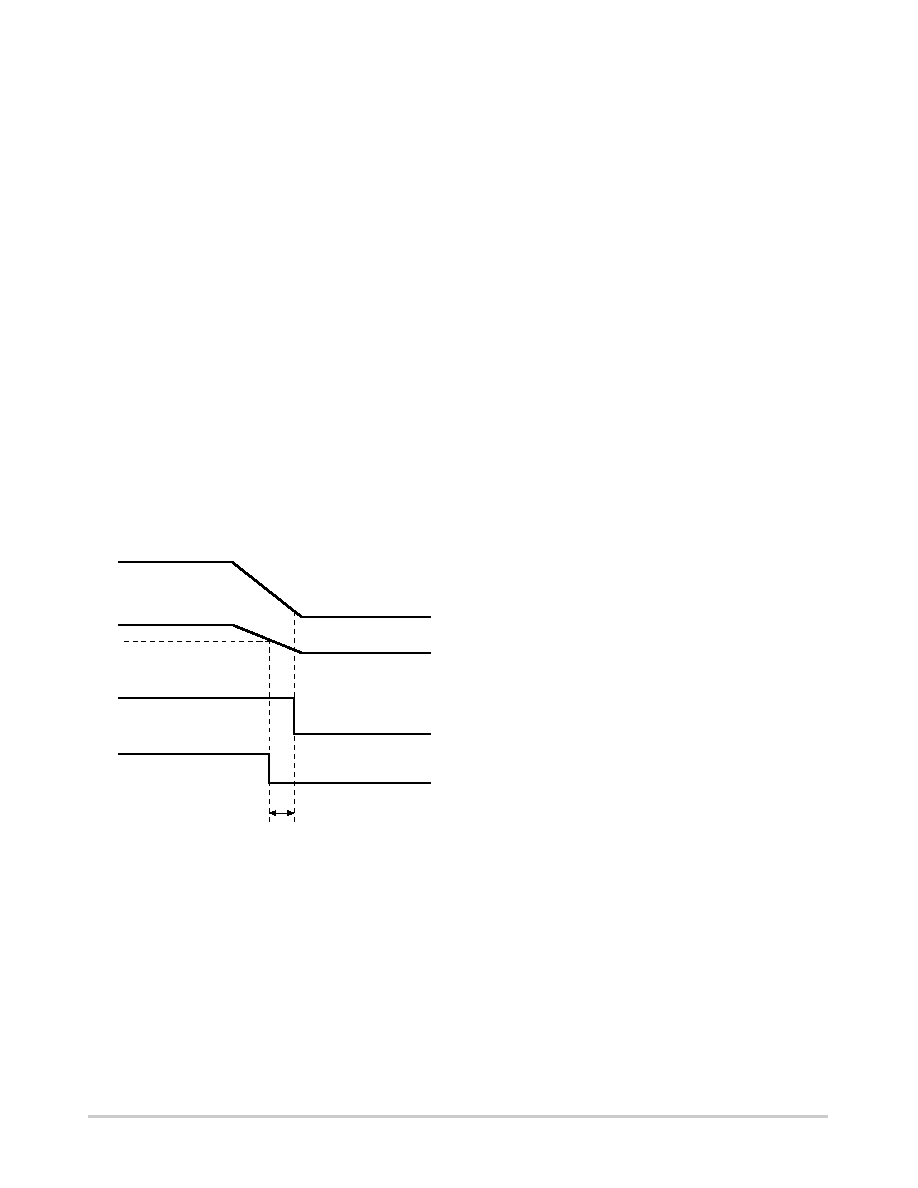
SIGNAL OUTPUT
Figure 21 shows the SO Monitor timing waveforms as a
result of the circuit depicted in Figure 20. As the output
voltage (VQ) falls, the monitor threshold (VSILOW), is
crossed. This causes the voltage on the SO output to go low
sending a warning signal to the microprocessor that a reset
signal may occur in a short period of time. TWARNING is the
time the microprocessor has to complete the function it is
currently working on and get ready for the reset
shutdown signal. When the voltage on the SO goes low and
the RO stays high the current consumption is typically
560
mA at 1 mA load current.
Figure 21. SO Warning Waveform Time Diagram
VQ
SI
VRO
VSI,Low
TWARNING
SO
STABILITY CONSIDERATIONS
compensating input line reactance. Possible oscillations
caused by input inductance and input capacitance can be
damped by using a resistor of approximately 1.0
W in series
with CI.
The output or compensation capacitor helps determine
three main characteristics of a linear regulator: startup delay,
load transient response and loop stability.
The capacitor value and type should be based on cost,
availability, size and temperature constraints. The
aluminum electrolytic capacitor is the least expensive
solution, but, if the circuit operates at low temperatures
(25
°C to 40°C), both the value and ESR of the capacitor
will vary considerably. The capacitor manufacturer’s data
sheet usually provides this information.
The 10
work for most applications; however, it is not necessarily the
optimized solution. Stability is guaranteed at CQ is min
2.2
mF and max ESR is 10 W. There is no min ESR limit
which was proved with MURATA’s ceramic caps
GRM31MR71A225KA01 (2.2
mF, 10 V, X7R, 1206) and
GRM31CR71A106KA01 (10
mF, 10 V, X7R, 1206) directly
soldered between output and ground pins.
CALCULATING POWER DISSIPATION IN A SINGLE
OUTPUT LINEAR REGULATOR
The maximum power dissipation for a single output
regulator (Figure 20) is:
PD(max) + [VI(max) * VQ(min)]IQ(max) ) VI(max)Iq (eq. 4)
where:
VI(max) is the maximum input voltage,
VQ(min) is the minimum output voltage,
IQ(max) is the maximum output current for the application,
and Iq is the quiescent current the regulator consumes at
IQ(max).
Once the value of PD(max) is known, the maximum
permissible value of RqJA can be calculated:
(eq. 5)
RqJA = (150°C – TA) / PD
The value of RqJA can then be compared with those in the
package section of the data sheet. Those packages with RqJA’s
less than the calculated value in equation 2 will keep the die
temperature below 150
°C. In some cases, none of the packages
will be sufficient to dissipate the heat generated by the IC, and
an external heatsink will be required. The current flow and
voltages are shown in the Measurement Circuit Diagram.
HEATSINKS
A heatsink effectively increases the surface area of the
package to improve the flow of heat away from the IC and
into the surrounding air.
Each material in the heat flow path between the IC and the
outside environment will have a thermal resistance. Like
series electrical resistances, these resistances are summed to
determine the value of RqJA:
RqJA + RqJC ) RqCS ) RqSA
(eq. 6)
where:
RqJC = the junctiontocase thermal resistance,
RqCS = the casetoheat sink thermal resistance, and
RqSA = the heat sinktoambient thermal resistance.
RqJC appears in the package section of the data sheet. Like
RqJA, it too is a function of package type. RqCS and RqSA are
functions of the package type, heatsink and the interface
between them. These values appear in data sheets of
heatsink
manufacturers.
Thermal,
mounting,
and
heatsinking considerations
are
discussed
in
the
ON Semiconductor application note AN1040/D, available
on the ON Semiconductor website.
相關PDF資料 |
PDF描述 |
|---|---|
| NCV4279A50D1R2G | 5 V / 150 mA LDO w/ Reset, Delay, Adjustable Reset and Early Warning |
| NCV4279CD1R2 | 5 V FIXED POSITIVE LDO REGULATOR, 0.6 V DROPOUT, PDSO8 |
| NCV4279CD1 | 5 V FIXED POSITIVE LDO REGULATOR, 0.6 V DROPOUT, PDSO8 |
| NCV4279CD2R2 | 5 V FIXED POSITIVE LDO REGULATOR, 0.6 V DROPOUT, PDSO14 |
| NCV4279CD2 | 5 V FIXED POSITIVE LDO REGULATOR, 0.6 V DROPOUT, PDSO14 |
相關代理商/技術參數(shù) |
參數(shù)描述 |
|---|---|
| NCV4279A50D1R2G | 功能描述:線性穩(wěn)壓器 - 標準 5.0V 150MA LDO RoHS:否 制造商:STMicroelectronics 輸出類型: 極性: 輸出電壓:1.8 V 輸出電流:150 mA 負載調節(jié): 最大輸入電壓:5.5 V 線路調整率: 最大工作溫度:+ 125 C 安裝風格:SMD/SMT 封裝 / 箱體:SOT-323-5L |
| NCV4279A50D2G | 功能描述:低壓差穩(wěn)壓器 - LDO 5.0V 150MA LDO RoHS:否 制造商:Texas Instruments 最大輸入電壓:36 V 輸出電壓:1.4 V to 20.5 V 回動電壓(最大值):307 mV 輸出電流:1 A 負載調節(jié):0.3 % 輸出端數(shù)量: 輸出類型:Fixed 最大工作溫度:+ 125 C 安裝風格:SMD/SMT 封裝 / 箱體:VQFN-20 |
| NCV4279A50D2R2G | 功能描述:低壓差穩(wěn)壓器 - LDO 5.0V 150MA LDO RoHS:否 制造商:Texas Instruments 最大輸入電壓:36 V 輸出電壓:1.4 V to 20.5 V 回動電壓(最大值):307 mV 輸出電流:1 A 負載調節(jié):0.3 % 輸出端數(shù)量: 輸出類型:Fixed 最大工作溫度:+ 125 C 安裝風格:SMD/SMT 封裝 / 箱體:VQFN-20 |
| NCV4279B | 制造商:ONSEMI 制造商全稱:ON Semiconductor 功能描述:5.0 V Micropower 150 mA LDO Linear Regulator with DELAY, Adjustable RESET, and Monitor FLAG |
| NCV4279BD1 | 制造商:ONSEMI 制造商全稱:ON Semiconductor 功能描述:5.0 V Micropower 150 mA LDO Linear Regulator with DELAY, Adjustable RESET, and Monitor FLAG |
發(fā)布緊急采購,3分鐘左右您將得到回復。